E-mail:szbldpcb@163.com
Hotline number:0755-26652383
E-mail:szbldpcb@163.com
Hotline number:0755-26652383

Time:2025-06-28Browse: 1179
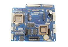
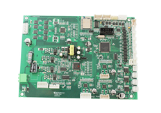
The complete process of PCB (printed circuit board) from design to production is usually divided into three stages:Design phase, manufacturing phase, and assembly phaseThe following is a detailed process description:
Requirement analysis and planning
Determine the circuit function, number of layers (single/double/multiple), size, materials (FR-4, high-frequency materials, etc.), and special requirements (impedance control, heat dissipation, etc.).
schematic design
Use EDA tools such as Altium Designer, KiCad, Cadence to draw circuit schematics and define component connection relationships.
PCB Layout
Component placementConsider signal integrity, heat dissipation, and electromagnetic compatibility (EMC).
wiringConnect component pins according to design rules (line width, spacing, via size).
Key design points:
High speed signals require equal length wiring;
Thickening or laying copper on power/ground wires;
High frequency circuits require impedance matching.
Design Rule Check (DRC)
Use EDA tools to automatically check for issues such as short circuits, broken wires, and spacing violations.
Generate production files
gerber filesImage files of each layer of copper foil, silk screen printing, and solder mask.
Drill FileIdentify the coordinates and aperture of the hole (in Excellon format).
BOM ListComponent model, quantity, and tag number.
Assembly drawingExplanation of component location and orientation.

material preparation
Select substrate (such as FR-4), copper foil (usually 1oz/2oz thickness), and cut according to the design size.
Inner layer production (suitable for multi-layer boards)
Pattern TransferTransfer the inner circuit pattern onto a copper plate through photolithography process.
etchUse chemical solution to remove excess copper foil and preserve the circuit.
AOI INSPECTIONAutomatic optical detection of circuit defects.
lamination
Stack the inner layer board, semi cured sheet (PP sheet), and copper foil, and press them together at high temperature and high pressure to form a multi-layer board.
drill
Drill through holes and blind buried holes with a CNC drilling machine, and clean the hole walls (remove adhesive residue).
Hole metallization (copper deposition)
By chemical deposition (copper deposition) and electroplating, the hole walls are made conductive, forming channels for conducting interlayer circuits.
Pattern imaging
Graphic transfer and etching (same as the inner layer) form the outer layer circuit.
Solder mask
Cover with insulating ink such as green/black, leaving only the solder pads exposed to prevent short circuits during soldering.
Silkscreen layer
Printing component identification Logo、 Polarity symbols and other white/yellow text.
Surface Treatment
Solder pad coating protective layer, commonly used process:
Spray Tin (HASL)Low cost, suitable for ordinary boards.
Sinking Gold (ENIG)High flatness, suitable for precision solder pads.
Immersion SilverHigh frequency signals are applicable.
OSP (organic solder mask)Environmentally friendly, but with a short shelf life.
Forming and Testing
Shape cuttingUse a milling machine or V-Cut to divide the board.
Electrical testing (flying needle/needle bed testing)100% detection of circuit conductivity.
Final inspectionSize, appearance, impedance sampling (high-speed board requires TDR testing).
SMT surface mount technology
Solder paste printingApply solder paste onto the solder pads through a steel mesh.
MounterMount resistors, capacitors, ICs, etc. onto solder pads.
Reflow SolderingMelting solder paste at high temperature to fix components.
THT plugin (through-hole technology)
Manually or machine inserted plug-in components (such as electrolytic capacitors, connectors).
Wave solderingWeld the plug-in pins through a molten tin furnace.
Mixed process (SMT THT)
Double sided panels may require SMT followed by THT, or step-by-step soldering on each side.
Manual welding and repair
Special components (large size, thermal sensitivity) require manual welding, and defective products need to be repaired.
Cleaning (optional)
Use ultrasonic waves or solvents to remove solder residue (necessary for military/medical boards).
Testing and Quality Inspection
ICT testingDetect component welding and parameter values.
FCT testingSimulate actual functions and verify the overall performance of the machine.
AOI/X-RayAutomatically detect defects such as virtual soldering, offset, BGA bubbles, etc.
Three proof coating (optional)
Spray protective paint (moisture-proof, anti-corrosion), suitable for harsh environments.
Packaging and Delivery
Anti static packaging, accompanied by test reports and compliance certificates (such as UL, RoHS).
High density board (HDI)Laser drilling, hole filling and electroplating are required.
High frequency/RF boardStrict impedance control, using Rogers materials.
Flexible Printed Circuit (FPC)Using polyimide substrate, the production process varies greatly.
Design determines success or failureDFM (Design for Manufacturability) can avoid production issues such as too small vias and insufficient line spacing.
Document accuracyGerber/drilling file error directly leads to scrapping.
Small batch verificationIt is recommended to conduct 5-10 sample tests for the first production.
Communicate with manufacturersConfirm the process capability in advance (such as minimum line width/aperture, interlayer alignment accuracy).
Through the above process, a PCB can be transformed from a design draft to a circuit board that can be installed and used, usually requiring5-15 days(Complexity determines). It is recommended to choose a factory with ISO certification and track production nodes throughout the process.
Address: 5th Floor, Science and Technology Building, Xinghua Road, Fuyong, Bao'an District, Shenzhen
Mr. Zhong (Marketing Director) 13590338876
Miss Liu (Head of Business Department) 13570886571
Phone: 0755-26652383 27873199
Email: szbldpcb@163.com