E-mail:szbldpcb@163.com
Hotline number:0755-26652383
E-mail:szbldpcb@163.com
Hotline number:0755-26652383
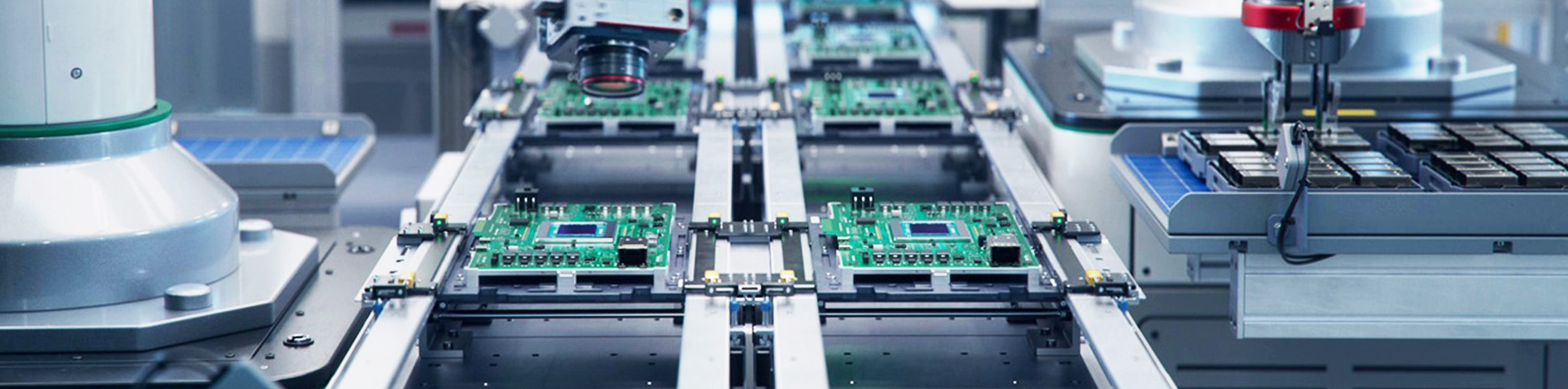
PCB Design functionality based on customer requirements. PCB Design Engineer Design PCB Schematic diagram to achieve the tasks requested by the customer. The main task of printed circuit board design is PCB The schematic design needs to consider the layout of external connections as well as the shape and structure of the product. In addition, PCB Board design needs to be considered PCB The optimal form of internal electronic components, circuit connections, and PCB The optimal layout of through holes, electromagnetic protection, and heat dissipation factors. Excellent printed circuit board design can save PCB Manufacturing costs and improving the performance of electronic products.
PCB Design services are ipcb One of the channels to help customers enter the market faster, because ipcb The company's PCB The board design engineering team is designing PCB Has rich practical experience in improving performance and manufacturability. IPCB Focusing on printed circuit board design in fields such as network communication, industrial control, medical, aerospace, etc; IC ATE Testing, computers, servers, automotive electronics, devices, and mobile phones.
What is? PCB Design?
If you are just an idea or concept, or have already completed a schematic, we can convert it into a design file and then proceed PCB Manufacturing PCB Assembly and testing. With over 15 years of experience in printed circuit board manufacturing and vehicle body design, we can ensure that the design fully meets manufacturing requirements.
2.IPCB of PWB The design team will collaborate with you throughout the entire product development process to ensure a technical review of all design aspects prior to initial production.
Once the printed circuit board design is approved for production, iPCB A skilled production team will be on standby to build high-quality products for preliminary testing and development purposes PCBA Prototype.
4. By machine and manual placement, parts can be filled in just 48 hours PCB Conduct a comprehensive inspection according to the standards and conduct additional tests as required.
5.iPCB Intended to provide all these services under one roof, making the process as seamless as possible and saving you valuable time to focus on bringing your products to market.

PCB design
iPCB Circuit board design - presenting you with perfect "layout" electronic art
Based on circuit board design and PCB Prototype manufacturing services, actively creating PWB Design PCB Manufacturing SMT One stop shop for chips and data PCB Assembly business.
senior PCB Design and PCB Layout Team
More than 15 years of professional design experience, from PCB Board design to PCBA Manufacturing provides solutions. The best circuit board design is "design quality", "cost control", and "easy debugging".
Experience in designing high difficulty printed circuit boards
Proficient in high frequency PCB、 high speed PCB、 high density PCB、 Mixed signal, high power, high current, RF PCB、ate PCB、 Combining rigidity and flexibility PCB、 High speed backboards, etc. 2000 per year PCB Board design experience.
Abundant technological resources
Chip companies cooperate early, accumulate forward-looking technology, synchronize cutting-edge technology, grasp the most advanced technology information, and fully consider EMI、EMC And manufacturability design.
High quality control system
Standardized design management system, strict control, layer by layer inspection, not letting go of any errors and details, ensuring zero failure rate, accumulating 10000 customer account monuments.
High standard safety measures
High standard confidentiality measures have been implemented, confidentiality agreements have been signed, and the company's designer computers are fully encrypted. The export of files requires full permission to ensure 100% confidentiality of the files.
Quality: Comprehensive "design guidelines" and "design specifications" provide PCB Additional technological suggestions beyond the layout, first-class training system, and training platform.
Self check: self check layout, wiring, rules, aesthetics, thermal design structure, etc
Review: ipcb The senior team participates in the research together, from schematic design DFM、DFT、 High speed EMC、 Conduct comprehensive inspections and mutual checks on thermal design and other aspects
Mutual inspection: avoid individual thinking patterns, brainstorming, standardized and strictly controlled joint inspection system, and improve DFM The best channel for reviewing the process
| |
PCB Design parameters Top 42 L Minimum line width 2.4 mil Maximum number of pins 110000 Maximum number of connections 78000 minimum BGA Pin spacing 0.3 mm BGA The maximum number of pins is 2912 Maximum speed signal 60 GHZ Minimum line spacing 2.4 mi |
PCB Design delivery date PIN Design delivery date 3-5 days within 1000 2000-3000 5-7 days 4000-5000 8-12 days 6000-7000 12-15 days 8000-9000 15-18 days 10000-13000 18-20 days 14000-15000 20-22 days 16000-20000, 22-30 days |
PCB Board design software
1.Protel、Protel 99SE、Protel-DXP and Altium Mainly used in China. These are software developed and upgraded by a company. The current version is Altium designer 15, It is relatively random and simple in design, but complex in production PCB The software is not very good.
2.Cadence SPB software Cadence SPB This is Cadence The current version of the software is Cadence SPB 16.5; OrCAD The schematic design is an international standard; PCB The design and simulation of the board are complete, which is more than Protel More complex, mainly due to complex requirements and settings; However, it provides regulations for design, so design can achieve twice the result with half the effort Protel More effective.
3.mentor The company's Bordestationg and ee, Among them, due to word station Only applicable to UNIX System, therefore not for PC Designed, therefore few people use it; mentor EE The current version is mentor EE 7.9 and cadence SPB, They belong to the same level PWB Design software. In some places, it is more cadence SPB Even worse. Its strength lies in pulling and flying wires, and it is known as the king of flying wires.
4.Eagle Easy to layout circuit board design is the most widely used printed circuit board design software in Europe. above-mentioned PWB Design software is widely used. Cadence SPB My mentor is undoubtedly the king. If you are a beginner in circuit board design, I think cadence SPB Better. It can give designers a good design habit and ensure good design quality.
How to design PCB Board? PCB The Four Stages of Design
1. Refine the concept - We have summarized the project objectives and created a document to specify the technological scope of the project.
2. Feasibility Study - We conducted a study to examine whether the project could be completed within the client's budget. List the agreed terms of reference. Submit a draft report to the client for feedback.
3. Hardware and software design - We design electronic circuits and create schematics, and manufacture desktop prototypes. The software code has been drafted.
4. Testing and experimentation - Once the software and hardware design is completed, we can begin serious bench testing. We will continue until the design meets the project specifications.
preparation in advance
Including the preparation of component libraries and schematics. Before designing the circuit board, a schematic diagram should be prepared first SCH Component library and PCB Component packaging library.
PCB It is best for engineers to build the component packaging library based on the standard size data of the selected devices. In principle, the first step is to establish PC Package the component library and then create a schematic diagram SCH Component library.
PCB The requirements for component packaging libraries are very high, which directly affects PCB The installation. schematic diagram SCH The requirements for component libraries are relatively relaxed, but attention should be paid to the definition of pin attributes and their relationship with PCB The correspondence between component packaging libraries.
PCB Structure Design
Based on the size and mechanical positioning of the circuit board PCB Draw in the board design environment PCB Frame and place the required connectors, buttons/switches, screw holes, assembly holes, etc. According to the positioning requirements. Fully consider and determine the wiring area and non wiring area (how many areas around the screw hole are non wiring areas)
PCB design
Make according to the required product features PCB Schematic diagram, using PCB Schematic design tools draw schematic diagrams and generate corresponding network tables. Of course, in certain special cases, such as when the circuit board is relatively simple and has a netlist, it can directly enter the circuit board design system without the need for schematic design. In the printed circuit board design system, you can directly participate in packaging and manually generate network tables.
You can also manually modify the network table to define solder pads instead of in PCB On the schematic, for example, fixed pins of certain components are connected to the network they are connected to, while pads without any physical connection can be defined as grounded or protected grounded. Translate the schematic and PCB Some devices with inconsistent pin names in the packaging library have their pin names changed to match PCB The pin names in the packaging library are consistent, especially for diodes and transistors.
PCB layout
exist PCB Among them, there are some key components, core components, interference prone components, high-voltage components, high calorific value components, and some anisotropic components. The positions of these special components need to be carefully analyzed. PCB The layout conforms to the circuit function and PCB Manufacturing and PCBA Manufacturing requirements. Improper placement of these components may lead to circuit compatibility issues or signal integrity problems, resulting in circuit board design failures.
exist PCB When placing special components in board design, the first consideration should be PCB Size. Ipcb I believe that when PCB When the size is too large, the printing line becomes long, the impedance increases, the drying resistance decreases, and the cost increases; If it is too small and has poor heat dissipation, adjacent lines are prone to interference. In determining PCB After determining the size, determine the square position of the special component. Finally, all components of the circuit are evaluated based on their functional units PCB Layout.
PCB Sample production- PCB Assembly- PCBA board
This is a PCB The process of designing functions from samples to printed circuit boards. This process requires a professional manufacturing team to complete. For example, some errors in the process can also lead to the failure of product development, so this is a very important process.
Purchasing components, replacing compatible functional components, designing signal sources, testing racks, etc.
We promise to provide you with convenient and efficient services at any time with high-quality product quality, low prices, and comprehensive and timely technical support. We sincerely welcome you to consult and negotiate business.
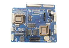
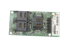
PCB The design mainly involves product categories
Network devices, Bluetooth devices C、Ku Band tuner, large router, digital camera, digital video recorder, other high-precision electronic products, laptop motherboard DVB、 Satellite receiver, wireless communication module PCB Motherboard, mobile phone PHS、 Interphone DVD、 Portable visual devices
PCB Design service advantages
1. Strong strength, senior experts
IPCB Our senior experts provide technical guidance and support to assist you PCB Design quality provides the strongest guarantee.
2. Strict processes and standardized guarantees
Strict design process, meticulous R&D team, perfect design standards, and classic cases will make your PCB Minimizing board design risks.
3. Thoughtful service and large team size
Software and hardware engineers who have been engaged in technology development and circuit board design for many years have fully built the best communication and powerful circuit board design team to meet customers' sudden needs in any situation
4. Having software to improve efficiency
A unique platform team has been established to develop tool software that fits the characteristics of the existing platform, significantly improving work efficiency and shortening time PCB Design cycle.
5. Keep up with the times
Closely monitor the latest developments in the industry, keep up with cutting-edge technologies, communicate closely with advanced technologies in the industry, and ensure the best guarantee for high-end printed circuit board design

PCB design process
In electronic design and development, attention should be paid to the design of printed circuit boards and the selection of electronic components.
1. Printed circuit board design should consider wiring SMT Difficulties, separation of analog and digital circuits, electromagnetic interference between components and circuits, and other related issues. Pay special attention to interference issues, as they are sometimes hidden problems that may arise at some point. If it appears after large-scale production, it would be embarrassing.
2. When selecting electronic components, side doors should be avoided as the component may face shutdown at any time or be difficult to be compatible with other components. Sometimes replacing components can cause a lot of trouble because the pins or drivers are incompatible. For products, using mature and stable components can not only improve product stability, but sometimes also reduce product costs.
PCB After the board design is completed, it can be carried out PCB Sample production. PCB After the sample is completed, firmware can be burned for testing and optimization PCBA。
IPCB The company's PCBA The advantages of design technology include manufacturability (DFM), testability (DFT), and assembly design (DFA)
high density B/B Circuit Board Design
Thermal considerations in printed circuit board design
Design process optimization
New design methods or technologies
PCB Stacking optimization design
Signal integrity simulation and analysis
In circuit board design EMC
power integrity
SI Application in actual product design
Specific products PCBA Design Technology
Design skills for processing power signals
PCB Teamwork in Board Design
EDA Advanced software features and applications
Introduce new layouts and simulations
IC Packaging Design Technology
Design considering cost reduction
IPCB It's a professional company PCB and PCBA Manufacturing company. We offer from PCB Designed to PCB Manufacturing PCB Assemble to complete R&D and production products. If you have a good idea, please contact us IPCB。
Address: 5th Floor, Science and Technology Building, Xinghua Road, Fuyong, Bao'an District, Shenzhen
Mr. Zhong (Marketing Director) 13590338876
Miss Liu (Head of Business Department) 13570886571
Phone: 0755-26652383 27873199
Email: szbldpcb@163.com