
PCB Layout Services
Benlida, EMS service provider
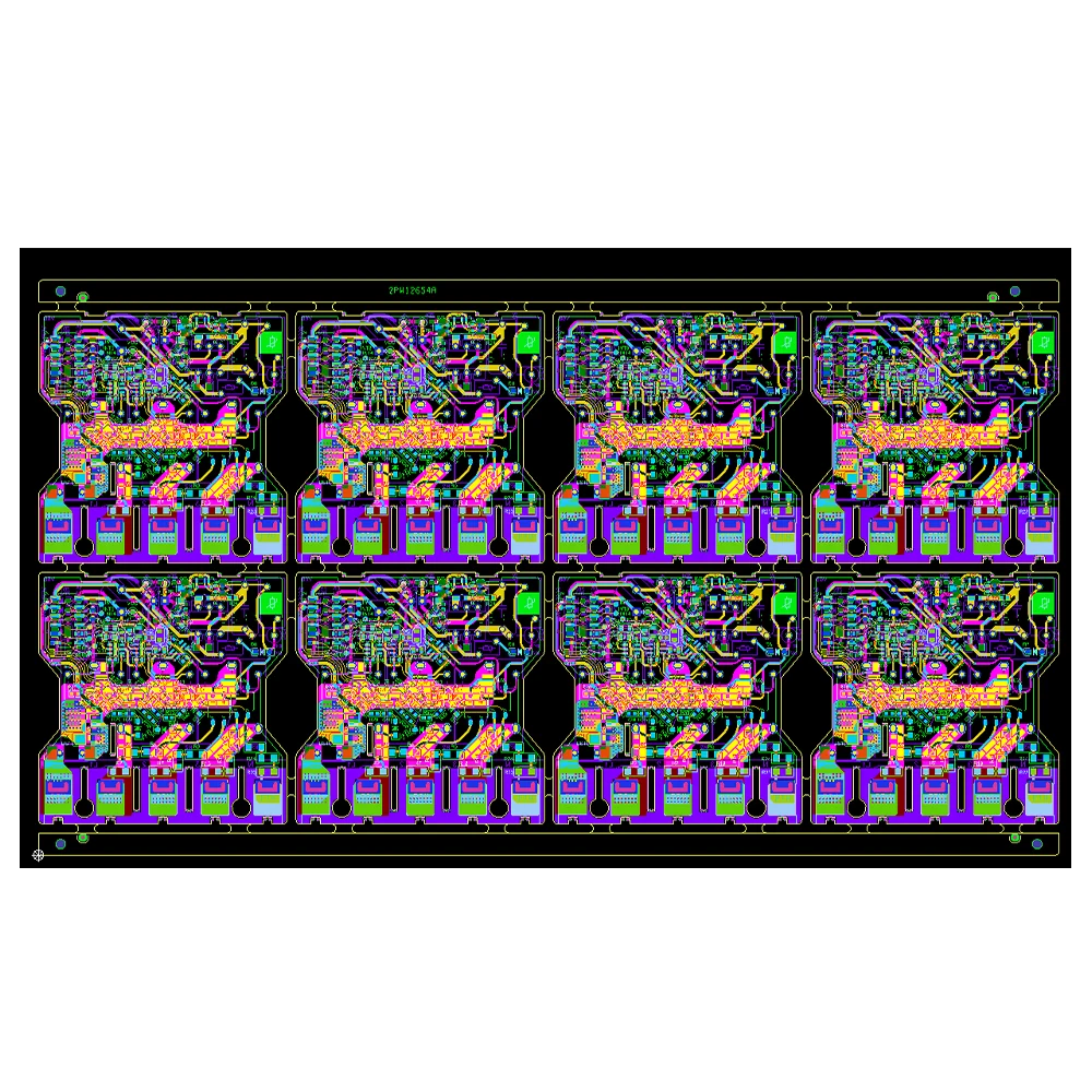
Benlida provides professional PCB Layout Services to convert complicated schematics into efficient, manufacturable PCB layout and routing. With our experienced engineers, sophisticated design techniques, and considerations of manufacturability, we support customers to have their own production files for high-speed, HDI, RF, power-supply, and other customized electronics.
Why Choose Benlida for for PCB Manufacturing?
Choose Benlida for precision PCB and PCBA manufacturing—delivering fast turnaround, consistent quality, and reliable performance from prototype to production.
Experienced Manufacturing
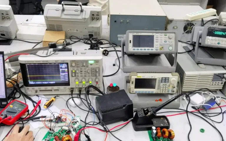
18 years of PCB manufacturing experience. Authoritative manufacturing team delivering consistent quality at every scale.

Advanced Quality Control
Comprehensive inspection processes including AOI, X-ray, and functional testing ensure every board meets the highest standards.

Fast Turnaround
Flexible production schedules with rapid prototype delivery. From design to finished PCB in record time without compromising quality.

Global Supply Chain
Trusted component sourcing from verified suppliers worldwide, ensuring authenticity and availability for every project.
Experienced Manufacturing
15 years of PCB manufacturing experience. Authoritative manufacturing team delivering consistent quality at every scale.
Advanced Quality Control
Comprehensive inspection processes including AOI, X-ray, and functional testing ensure every board meets the highest standards.
Fast Turnaround
Flexible production schedules with rapid prototype delivery. From design to finished PCB in record time without compromising quality.
Global Supply Chain
Trusted component sourcing from verified suppliers worldwide, ensuring authenticity and availability for every project.
Our Advantages in PCB Layout Design
Engineering-Driven PCB Layout Solutions for Reliable Manufacturing
PCB layout design is much more than just placing components and connecting them. One needs to know about signal integrity, power integrity, thermal management, and manufacturability issues. Benlida offers its clients dependable PCB Layout Services by integrating its knowledge about PCB design and manufacturing processes.
Manufacturing-Oriented Design Approach
Unlike independent design providers, Benlida integrates PCB layout experience with PCB manufacturing knowledge. During the design process, our engineers factor in considerations such as fabrication requirements, assembly methods, and testing requirements to minimize production risks.
Advanced Signal Integrity Optimization
In electronic devices that operate at high speeds, incorrect routing can lead to signal loss, interference, or unstable performance. Our engineers optimize critical signals by means of controlled impedance and differential pair routing.
Flexible Layout Capability
Benlida supports different PCB structures, including standard rigid boards, HDI boards, flexible PCBs, and rigid-flex designs. Our PCB Layout Services provide customized solutions for applications ranging from compact consumer electronics to complex industrial systems.
Complete Engineering Support
From schematic review to final production files, our engineers provide technical support throughout the entire design process. This helps customers move efficiently from concept development to manufacturing.
PCB Layout Services We Provide
Complete PCB Design and Layout Solutions
Benlida offers comprehensive PCB Layout Services that convert electrical concepts into optimized PCB designs. Performance, reliability, and manufacturability are our engineers’ priorities while working on any project from a prototype through production.
Conversion of Schematic to PCB Layout
We turn schematic drawings into full PCB layouts through proper placement of components, design of routing pathways, and optimization of board construction.
This service includes:
• Component placement optimization
• PCB layer planning
• Signal routing
• Power and ground design
• Manufacturing file preparation
A well-designed layout ensures the PCB can achieve stable electrical performance and efficient production.
High-Speed PCB Design
High-speed circuits require precise routing strategies to maintain signal quality. Our PCB Layout Services support high-speed design requirements through controlled routing and signal integrity optimization.
Key considerations include:
• Differential pair routing
• High-speed signal management
• Crosstalk reduction
• Timing optimization
• Impedance control
RF and Impedance-Controlled Layouts
RF and communication products require careful control of electromagnetic performance. Benlida provides specialized layout solutions for RF circuits and impedance-sensitive designs.
Our engineers optimize:
• RF signal paths
• Transmission line structures
• Grounding methods
• Electromagnetic interference control
HDI PCB Design
High Density Interconnect (HDI) technology enables smaller and more powerful electronic products. Our layout engineers support HDI designs with advanced routing techniques and compact component placement.
HDI layout capabilities include:
• Microvia design
• Fine-pitch component placement
• Multi-layer optimization
• Space-efficient routing
Flexible and Rigid-Flex PCB Layout
Flexible PCB designs require special consideration for bending areas, mechanical constraints, and reliability. Benlida provides layout solutions for flexible and rigid-flex applications.
Power Electronics PCB Layout
Power circuits require effective current distribution and thermal management. Our engineers optimize power PCB layouts for:
• High-current applications
• Power supply systems
• Heat dissipation requirements
• Voltage isolation design
Comprehensive PCB Design and Layout Capabilities
Supporting Different Electronic Design Requirements
Benlida provides complete PCB Layout Services covering various technical requirements. Our engineering team combines design experience with manufacturing knowledge to create reliable PCB solutions for different industries.

High-Speed Digital PCB Design
High-speed digital products require accurate routing and signal control. Through professional PCB Layout Services, Benlida helps optimize high-speed designs to maintain stable operation for advanced electronic systems.
Our engineers optimize:
• Differential signals
• Clock routing
• Data transmission paths
• Signal timing performance
RF and Microwave PCB Design
RF applications require precise electromagnetic control. This ensures reliable performance for wireless and communication products.
Our engineers focus on:
• RF routing optimization
• Impedance matching
• Noise reduction
• Signal isolation
High-Power and High-Voltage PCB Layout
Power electronics require special attention to safety and thermal performance. Benlida applies engineering experience to develop reliable layouts that meet demanding electrical requirements.
Design considerations include:
• Current carrying capability
• Heat management
• Clearance and creepage distance
• Power distribution optimization
HDI and Special PCB Design
For compact and advanced products, Benlida provides customized PCB layout solutions for HDI and special PCB designs. Our PCB Layout Services support complex structures requiring:
• High-density routing
• Multi-layer structures
• Miniaturized component integration
• Complex interconnection design
Our PCB Design Capabilities
Advanced Engineering Capability for Optimized PCB Layout
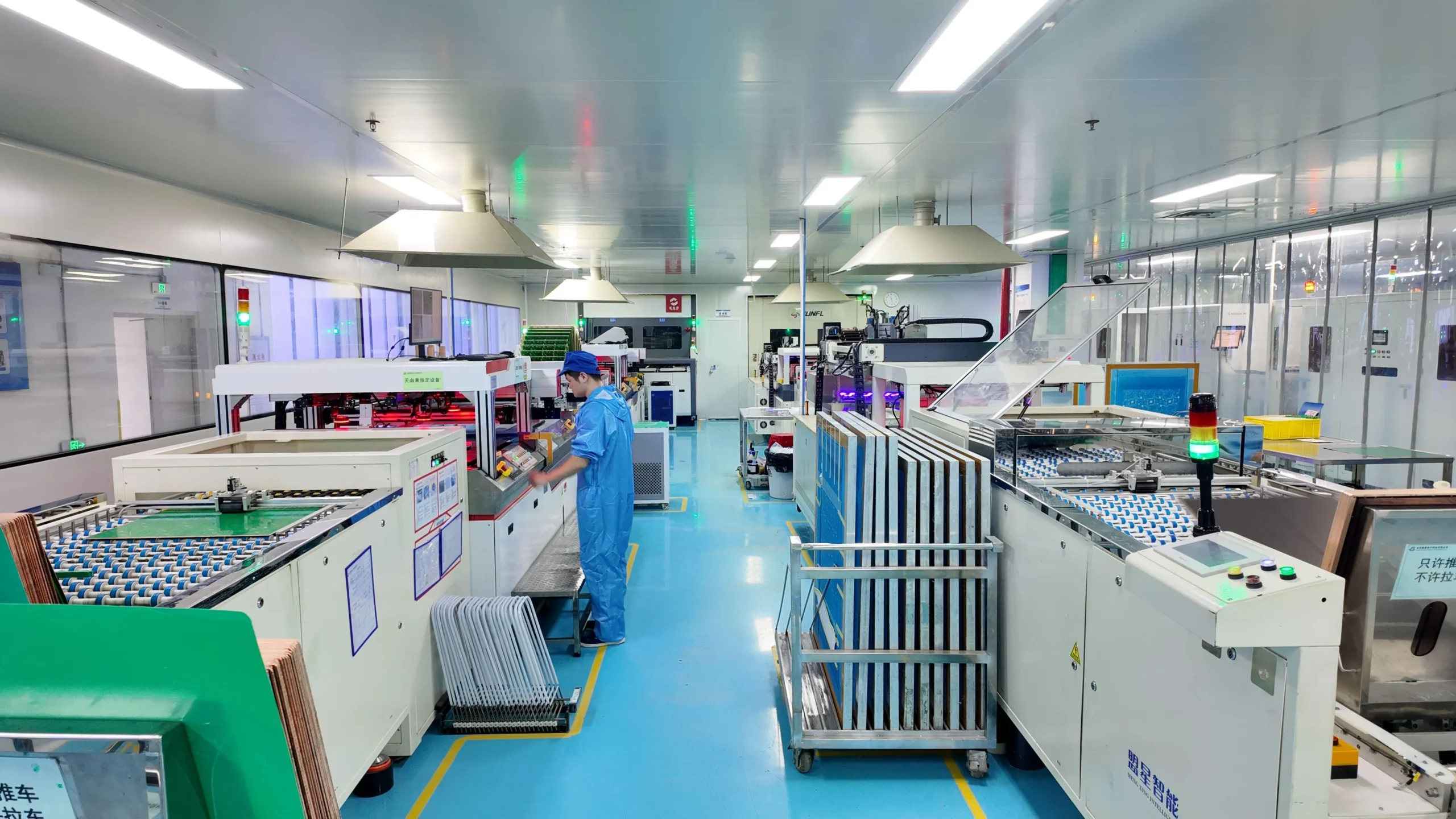
Benlida provides professional PCB design capabilities to support complex electronic products from initial concept to production preparation. Our PCB Layout Services focus on electrical performance, manufacturability, and long-term reliability during every design stage, helping customers develop stable and production-ready PCB solutions.
High-Speed Signal Routing
Optimize high-frequency and high-speed signal paths through controlled routing strategies to reduce signal loss and improve communication stability.
Controlled Impedance Design
Design accurate impedance structures according to signal requirements, helping maintain consistent transmission performance.
EMI/EMC Optimization
Apply proper grounding, shielding, and routing methods to reduce electromagnetic interference and improve product reliability.
Dense Component Placement
Optimize component arrangement for compact PCB designs while maintaining assembly efficiency and thermal performance.
Stack-Up Design and Material Selection
Develop suitable layer structures and material selections according to electrical, mechanical, and manufacturing requirements.
Design for Manufacturing & Assembly
Review PCB designs from a production perspective to improve manufacturability and reduce potential manufacturing issues.
PCB Layout Design Process
Complete Workflow from Requirement Analysis to Production Files
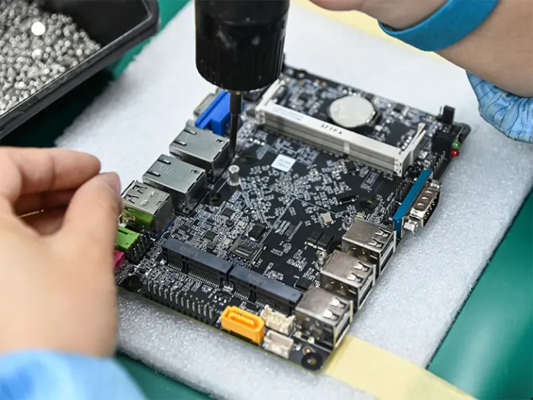
A reliable PCB layout process requires careful planning, engineering verification, and manufacturing consideration. Benlida provides professional PCB Layout Services to help customers transform circuit concepts into production-ready PCB designs. Through a structured workflow, our engineers ensure each layout achieves electrical performance, manufacturing feasibility, and stable production results.
Requirements & Feasibility
The PCB Layout Services process begins with a detailed review of product specifications, schematic files, performance requirements, and manufacturing conditions. Engineers analyze project requirements to create a suitable layout strategy.
This stage includes:
• Electrical requirement evaluation
• Component analysis
• Design feasibility checking
• Production requirement confirmation
1

Stack-Up & Placement
Benlida optimizes PCB layer structures and component placement based on signal, power, and mechanical requirements. Our PCB Layout Services focus on improving design reliability and ensuring efficient manufacturing.
Engineers optimize:
• Layer arrangement
• Component positioning
• Power distribution
• Thermal considerations
2

Routing & SI Optimization
Automotive systems require electronic products that can withstand vibration and temperature changes.
DIP technology is used in:
- Vehicle control modules
- Electronic control systems
- Sensor devices
- Power management equipment
Reliable DIP circuit board manufacturing helps improve product durability.
3

Simulation & Design Verification
Before manufacturing, simulation and verification are performed to evaluate PCB performance. These verification steps help ensure the final layout meets electrical and production requirements.
Verification includes:
• Signal integrity analysis
• Power integrity analysis
• Thermal analysis
• Electrical performance evaluation
4

DFM/DFA Review
Design for Manufacturing and Design for Assembly analysis ensure the PCB layout is ready for production. Benlida integrates manufacturing considerations into PCB Layout Services to reduce potential production issues.
Checks include:
• Manufacturing feasibility
• Component accessibility
• Assembly requirements
• Production optimization
5
Final Output & Documentation
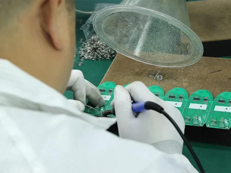
After design approval, complete production files are prepared for manufacturing. Benlida delivers accurate documentation to support smooth PCB fabrication and assembly.
Deliverables include:
• Gerber files
• ODB++ files
• BOM files
• Pick-and-place files
• Manufacturing documentation
6
PCB Solutions Across Industries
Benlida provides reliable PCB solutions for a wide range of industries, including consumer electronics, industrial automation, medical devices, automotive electronics, telecommunications, and aerospace applications. We deliver customized PCB solutions with stable performance and reliable quality to meet different application requirements.
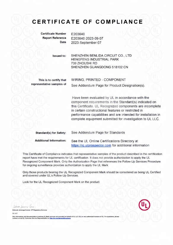
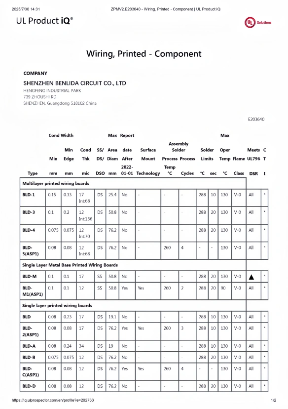
Our Certificates
Quality Standards Supporting Reliable PCB Design and Manufacturing
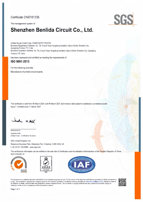
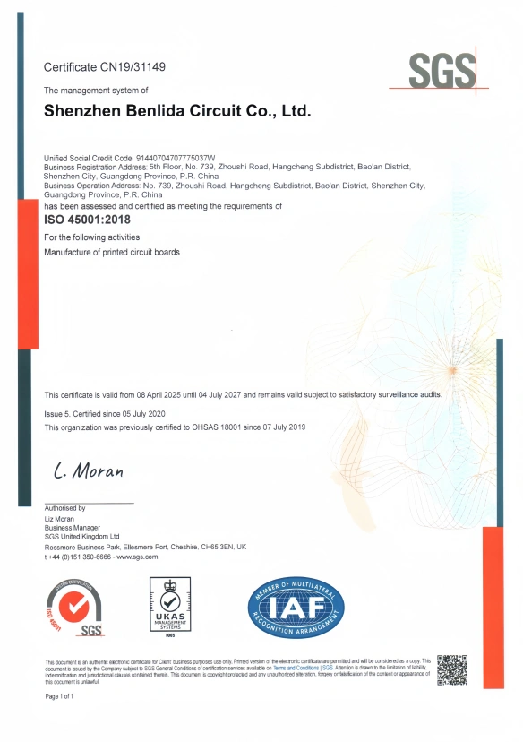
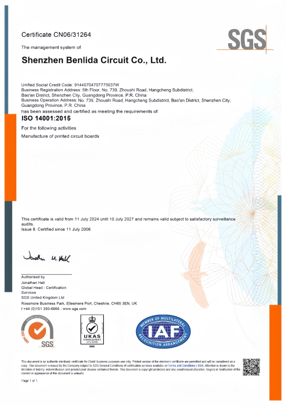
Benlida follows strict quality management systems throughout PCB design and manufacturing processes. Our certifications demonstrate our commitment to reliable production, environmental responsibility, and international quality requirements.
These standards help ensure that PCB projects designed through our PCB Layout Services can smoothly transition into reliable manufacturing. Our certification system includes:
• SGS Certification
• ISO-related quality management standards
• RoHS Compliance




FAQ
PCB Layout Services involve transforming circuit schematics into production-ready PCB designs through component placement, routing, layer planning, and design optimization.
Customers usually provide schematic files, BOM, PCB requirements, component information, and manufacturing specifications.
Yes. Benlida supports high-speed PCB design including impedance control, differential pair routing, and signal integrity optimization.
Yes. Our engineers support HDI PCB designs with microvia structures, high-density routing, and compact component placement.
Yes. Our engineers perform DFM/DFA reviews to ensure designs are suitable for PCB fabrication and assembly.
Yes. Benlida provides layout solutions that support the complete product development process from prototype verification to production manufacturing.