

Professional Multilayer PCB Manufacturer
Custom Multilayer PCB Manufacturing
Offering state-of-the-art fabrication services of multilayer PCB boards, up to 32 layers, controlled impedance, quick turnaround times, and global logistics.
Advanced lamination & stack-up engineering
Tight tolerance & high layer count capability
IPC-6012 Class 2 / Class 3
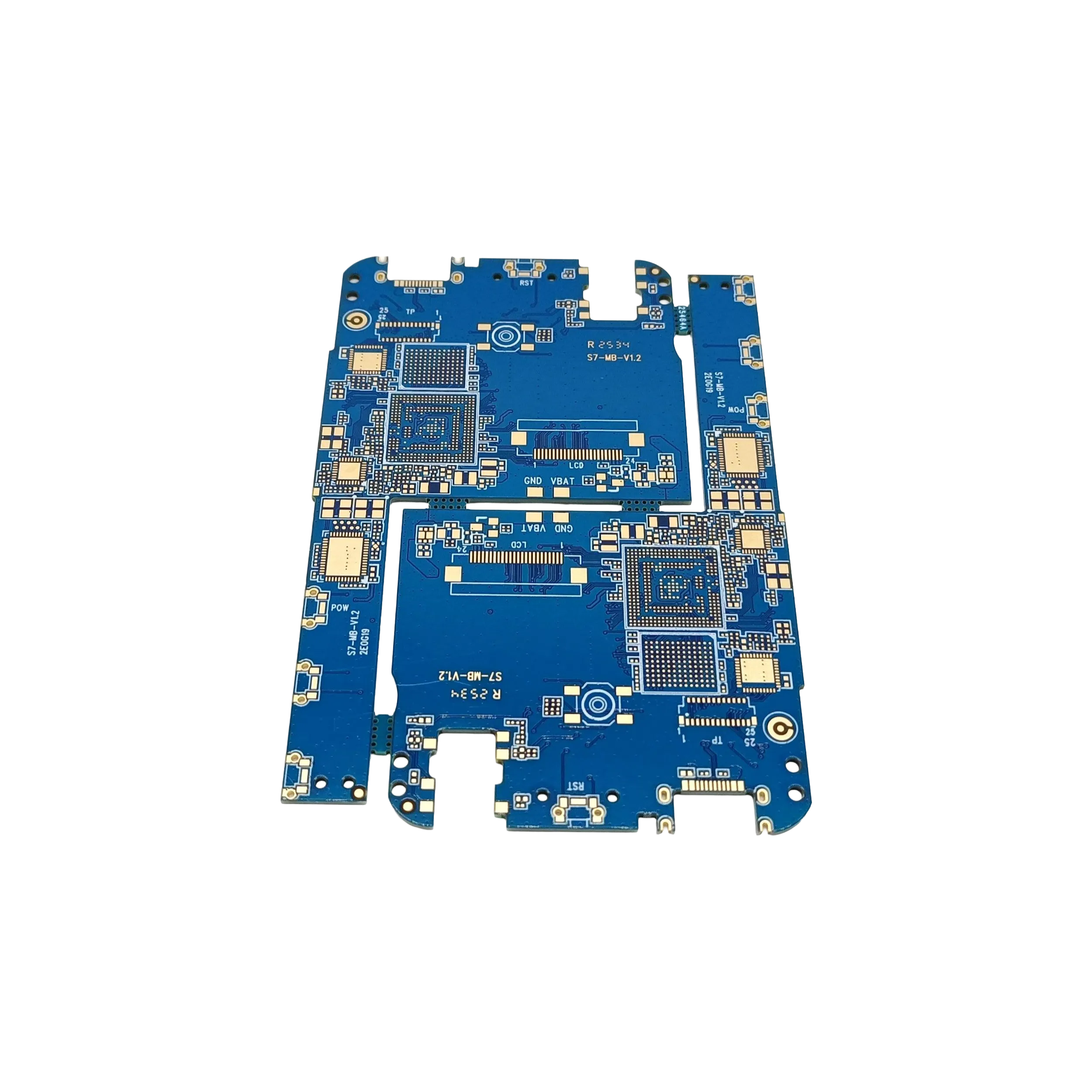
Our Multilayer PCB Manufacturing Capabilities
The capability table below summarizes the multilayer fabrication options presented on this page. Review the fields for layer count, trace/space, board thickness, materials, via size, impedance requirements, surface finishes, hole tolerances, and related options.
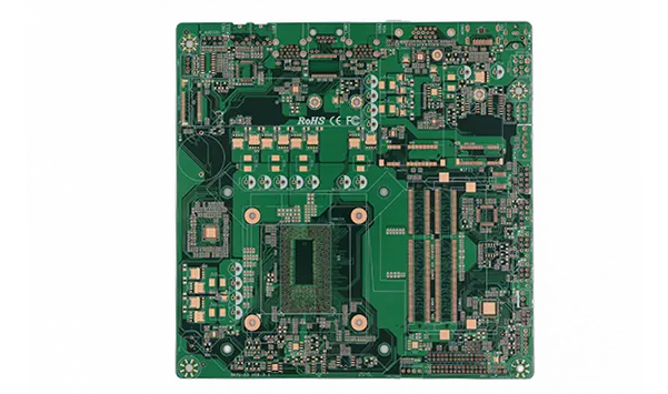
Layer Count
4–32 layers
Min Trace/Space
3/3 mil (0.075/0.075 mm)
Impedance Control
Targets and verification requirements are defined per project.
Surface Finish
HASL, lead-free HASL, ENIG, Immersion Silver
Hole Tolerance
Plated: +0.13/-0.08 mm; Non-plated: ±0.2 mm
OEM/ODM
available
Board Thickness
0.2–6.0 mm
Materials
FR-4, High-Tg, Rogers, Polyimide
Gold Finger / Bevel
Supported
Min Via Size
0.15 mm (hole) / 0.25 mm (pad)
MOQ
1 pcs
Packaging
ESD Protection Materials, Moisture barrier bags, Bubble wrap, Corrugated cartons
What is a Multilayer PCB?
Overview
A multilayer PCB combines three or more conductive copper layers with dielectric materials in one laminated construction. Its performance depends on the complete stack-up, material set, via structure, and manufacturing controls rather than layer count alone.
Inside the Board
It is more than a double-sided design with additional copper layers. The layer sequence, dielectric structure, copper distribution, registration, vias, and lamination process must work as an integrated construction.
Components are typically mounted on the outer surfaces, while inner layers may carry signals or provide power and ground references. Component placement and internal layer functions vary with the construction.
Related services and board types: Explore our PCB Manufacturing Services or review HDI PCB options for higher-density interconnect requirements. For component sourcing or assembly support, see our PCB Assembly Services.
Multilayer PCB Stack-Up Design and Lamination Services
A manufacturable stack-up connects electrical intent with real materials and process tolerances. Define the layer sequence, signal and reference planes, copper weight by layer, core and prepreg structure, target finished thickness, material grade, special vias, and controlled-impedance requirements. There is no universal stack-up that is correct for every design.
For builds that require higher copper weight for current-carrying paths, review our Heavy Copper PCB manufacturing capabilities.
Customized PCB Stack-Up Design
Design an optimized stack-up of PCB depending on its complexity and the number of layers, and on particular product requirements. Consider signal layers, power plane layers, ground plane layers, and mixed layers configurations.
Impedance Control and Signal Integrity Optimization
For impedance review, identify each single-ended or differential target, tolerance, signal layer, reference layer, trace geometry, and any coupon or report requirement. Design target, production adjustment, and measured result are separate records.
Reliable Multilayer PCB Lamination Process
For a multilayer construction, the cores, prepregs or bondplies, and copper foils are arranged according to the approved layer sequence and lamination plan. Pressed thickness, resin fill, and layer bonding depend on the selected materials, copper distribution, and process window. For hybrid constructions, the stack-up and process parameters depend on the selected material combination.
Full Engineering Support from Design to Manufacturing
Engineering support can include DFM analysis, stack-up optimization, and manufacturing recommendations during prototype validation and production planning.
Multilayer PCB Materials
Material selection for multilayer PCBs depends on the project’s electrical requirements and stack-up. If insertion loss, dielectric loss, or RF performance is a design constraint, specify the frequency range, transmission-line requirements, material-selection criteria, and verification method. Controlled impedance does not mean lossless transmission.
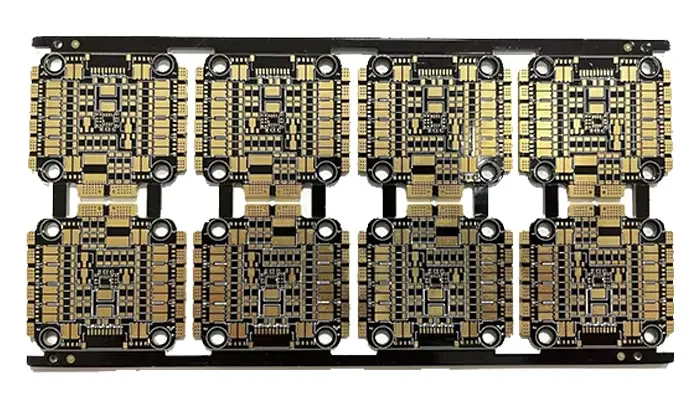
FR-4 High-Tg Materials
Suitable for multilayer PCB applications across different industries.
Good thermal stability, mechanical strength, and dimensional stability. Has many applications in industrial control systems, communication devices, and consumer electronics.
For FR-4 material selection and related manufacturing details, see our FR-4 PCB manufacturing page.
Rogers Materials in Multilayer Stack-Ups
When a project specifies Rogers materials, identify the exact material family and grade in the multilayer stack-up.
For frequency-dependent material behavior, loss, impedance, and related process considerations, see our High-Frequency PCB manufacturing page.
Polyimide for Rigid Multilayer Stack-Ups
For a rigid multilayer PCB, specify the exact polyimide laminate or prepreg system and complete stack-up. The material name alone does not define temperature range, reliability class, or end-use suitability.
Flexible polyimide film and flexible copper-clad laminate are used in flex or rigid-flex constructions and are not covered by this page. For bendable layers or rigid-flex stack-ups, see our Rigid-Flex PCB manufacturing page.
Mixed Material Lamination Solutions
Supports hybrid stack-up designs combining different PCB materials based on application requirements.
Maximizing the material based on the electrical performance, cost, and manufacturing considerations.
It can be used in high-layer counts and high-density multilayer PCB board constructions.
Low-Loss Requirements for Multilayer Stack-Ups
For a multilayer PCB, define low-loss requirements by operating frequency, transmission-line requirements, stack-up, and verification method.
Evaluate Dk and Df using the selected material grade and stated test conditions; generic low-Dk or low-Df labels do not define performance for every design.
Benlida can support material selection in the context of the complete stack-up and project requirements.
Multilayer PCB Manufacturing Process
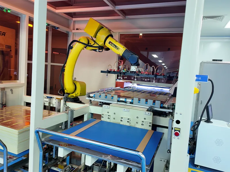
Benlida uses highly sophisticated multilayer PCB manufacturing technologies that include design evaluation, creation of inner layer circuitry, accurate lamination, drilling, electroless/electroplating, and final testing. By using our professional experience in layer pressing technology, we can control temperature, pressure, time, and alignment of layers during lamination to create a powerful bond between layers and ensure performance consistency in high-layered multilayer PCB board production.
1
Stack-Up Design & Engineering Review
Our engineers analyze the PCB design, layer configuration, material requirements, impedance control, and manufacturing specifications to develop a reliable multilayer PCB stack-up.

2
Inner Layer Circuit Formation
Circuit patterns are transferred onto the inner copper layers using precision imaging and etching processes to create accurate internal circuits for multilayer structures.
3
Layer Alignment & Registration Control
Each inner layer is carefully aligned using advanced registration technology to ensure precise layer positioning and reliable electrical connections throughout the PCB.
4
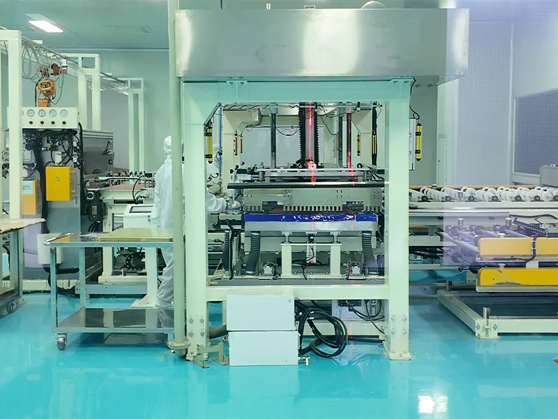
Multilayer Lamination Process
Inner layers are bonded together with prepreg materials under controlled heat and pressure, forming a solid multilayer PCB structure with strong mechanical stability.
5
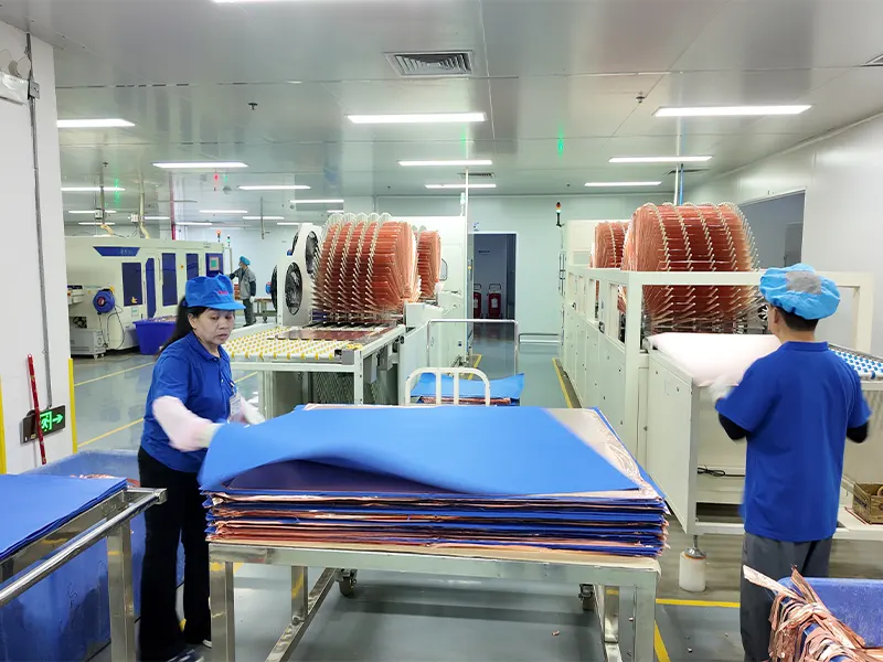
Drilling & Interlayer Connection
Precision drilling creates through holes and vias that connect different circuit layers, enabling efficient signal transmission and electrical performance.
6
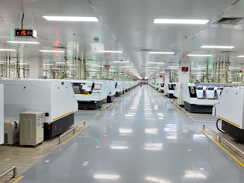
Copper Plating & Circuit Enhancement
Copper plating strengthens via walls and improves conductivity, ensuring stable connections between multiple PCB layers during long-term operation.
7
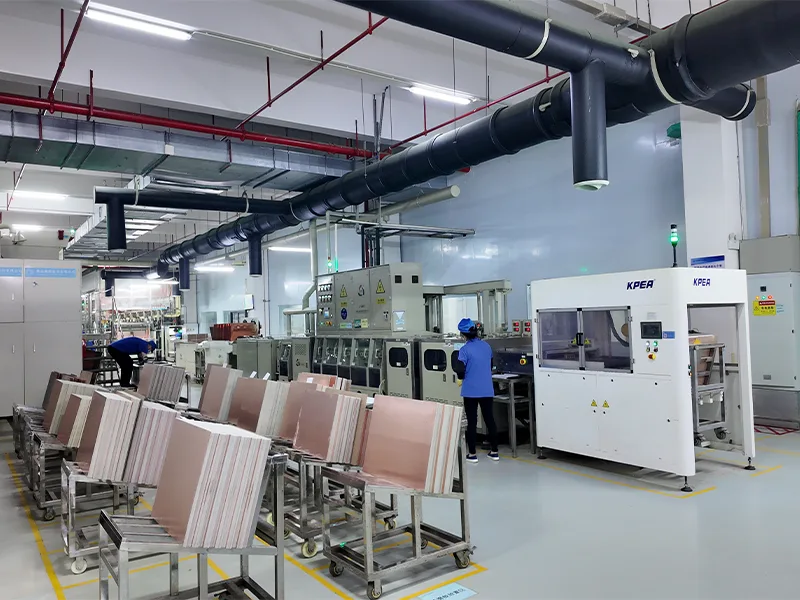
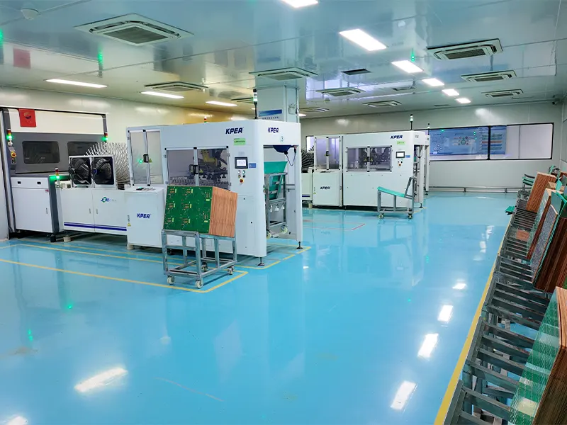
Surface Protection & Final Processing
Solder mask application, surface finishing, silkscreen printing, and profile processing are completed according to customer requirements.
8
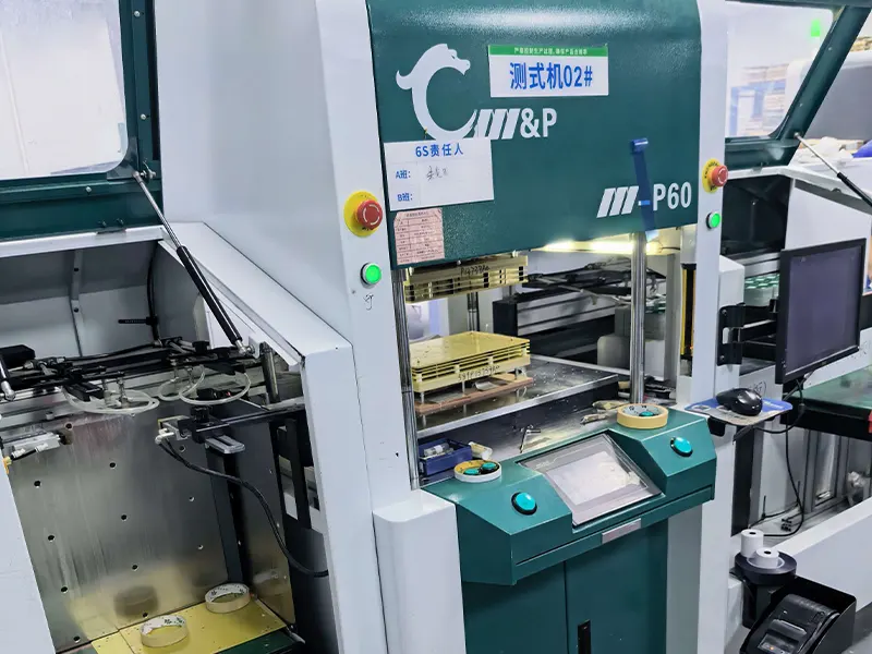
Electrical Testing & Quality Verification
Multilayer PCBs undergo electrical testing, layer inspection, and quality checks to ensure reliability, consistency, and compliance with industry standards.
What Tests Are Performed on Multilayer PCB Boards?
Benlida conducts comprehensive testing and inspection throughout the multilayer PCB board manufacturing process to ensure product quality, electrical performance, and long-term reliability. As an experienced multilayer PCB manufacturer, we apply strict testing procedures to identify potential defects and verify that each PCB meets customer requirements before delivery.
Electrical Testing
Perform continuity and isolation testing to verify circuit connectivity and prevent open or short circuit issues.
Ensure reliable electrical performance before shipment.
Automated Optical Inspection (AOI)
Inspect inner and outer layer circuits using advanced optical systems.
Detect potential defects such as line width variation, missing traces, and circuit abnormalities.
Impedance Testing
Impedance verification must use the method, sampling plan, acceptance criteria, and reporting requirements agreed for the order.
If the approved test plan specifies a representative coupon and TDR, the coupon design and measurement method must correspond to the production stack-up. A coupon or TDR result does not by itself prove loss, crosstalk, every routed net, or complete signal integrity.
For a practical explanation of impedance targets, stack-up inputs, and TDR verification, read our PCB impedance control guide.
X-Ray Inspection
Inspect hidden structures such as internal layers, vias, and complex connections.
Ensure accurate layer alignment and reliable internal bonding quality.
Solderability and Surface Finish Inspection
Check surface finish quality, including ENIG, HASL, and other finishes.
Ensure excellent solderability and long-term connection reliability.
Final Quality Inspection
Conduct final appearance checks, dimensional verification, and packaging inspection before delivery. Ensure products meet customer specifications and manufacturing standards.
Cost Factors & Optimization
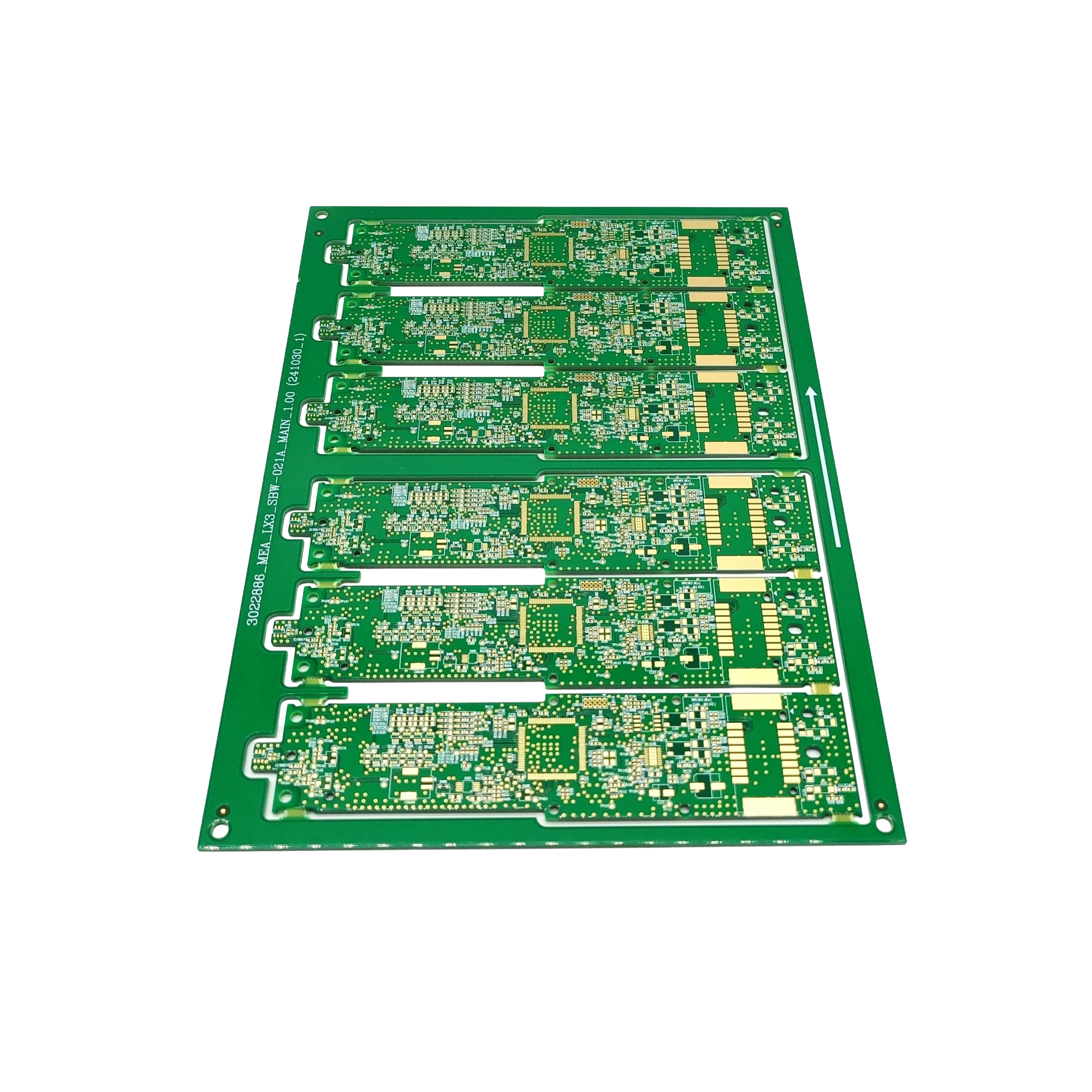
The price of a multilayer PCB board relies heavily on the number of layers, the material used, vias, and complexity, as well as other manufacturing aspects. As one of the best multilayer PCB manufacturers in the industry, Benlida helps its clients optimize their designs, select appropriate materials, and improve efficiency in production, while at the same time not affecting performance and price.
Layer Count
A larger number of layers means more materials are used, a more complicated manufacturing process, and a higher PCB manufacturing price. Proper stack-up design can help to balance performance demands and cost effectiveness.
Material Type
Special substrates and high-performance laminates may cost more, but will ensure better electrical performance and stability of the PCB.
Via Complexity
Advanced via structures can change the build sequence, drilling, metallization, inspection, cost, and lead-time requirements. Define the layer span, drill method, geometry, fill and cap, and verification requirements for each applicable structure, including blind or buried vias, laser microvias, via-in-pad, sequential build-up, and backdrill. Neither layer count nor the presence of blind or buried vias is enough by itself to define an HDI construction. A single via diameter is also not a complete capability definition.
For a type-by-type comparison before choosing a via structure, read our PCB via types guide.
For backdrill, specify the drill side, layer pair, primary and backdrill diameters, target residual stub, depth tolerance, keepout, and verification method. For laser microvias, stacked or staggered structures, sequential build-up, and other HDI-specific questions, see our HDI PCB manufacturing page.
Yield Challenges
High density and narrow manufacturing tolerances can influence product yield. Professional control and optimization of processes minimize defects and reworks and unnecessary expenses.
Why Choose Benlida for Multilayer PCB Manufacturing
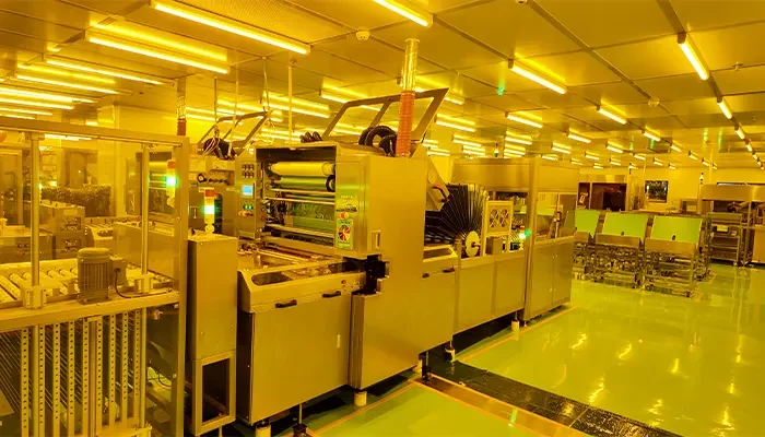
Extensive Multilayer PCB Manufacturing Experience
Benlida specializes in high-quality multilayer PCB board manufacturing, supporting 1–32 layer PCB production with the capability to handle complex designs, from rapid prototypes to high-volume production.
Professional Engineering Support and Design Optimization
Benlida’s engineering team offers services related to stack-up, impedance, DFM analysis, and manufacturing suggestions.
Strict Quality Control Process
From material choice and lamination through final testing, Benlida implements strict quality control procedures to ensure stable electrical performance, good quality, and reliability.
Flexible Production Capacity and Fast Delivery
Following strict quality control methods in all stages of production, Benlida ensures good electrical stability and reliable quality of its multilayer PCBs.
Complete PCB Manufacturing Solutions
Benlida supports the fabrication workflow from initial design review through production.
FAQ
For a multilayer PCB quote, provide Gerber or ODB++ data, NC Drill data, a fabrication drawing, revision, quantity, layer count, finished thickness, copper weight by layer, and surface finish. When applicable, also include the stack-up, exact material grade, impedance targets, special-via details, tolerances, test requirements, and requested delivery date.
This page lists Benlida’s multilayer PCB range as 4–32 layers. Feasibility within that range also depends on finished thickness, copper distribution, trace and space, hole and via structure, and material system. Lamination cycles, panel size, impedance requirements, testing, quantity, and delivery target also matter. Submit the current fabrication package so the build can be checked and quoted.
Yes. Benlida can review a customer-supplied stack-up or propose a manufacturable stack-up for the project. The review considers layer sequence, signal and reference planes, copper weight by layer, core and prepreg structure, finished thickness, material choice, via construction, impedance targets, and manufacturing tolerances. The production stack-up and current fabrication revision should be approved before manufacture.
Define each single-ended or differential impedance target, tolerance, signal layer, reference layer, and trace type in the project data. These inputs are checked against the production stack-up, selected material data, copper, and manufacturing tolerances. When coupon and TDR verification are included, the coupon design and measurement method should correspond to the approved production stack-up.
This page lists a minimum via of 0.15 mm hole with a 0.25 mm pad. State the required via type and measurement basis in the design package. For blind or buried vias, laser microvias, via-in-pad, sequential build-up, filled or capped vias, and backdrill, provide the applicable layer span and structure details. See the HDI PCB page for HDI-specific builds.
Material categories shown on this page include FR-4, high-Tg, Rogers, and polyimide. Identify the exact manufacturer and grade, then match the selection to the project’s electrical, thermal, mechanical, stack-up, and availability requirements. Different Rogers families are not interchangeable, and rigid polyimide laminates are not the same as flexible polyimide film. Hybrid constructions depend on the selected material combination and lamination route.
Inspection options shown on this page include bare-board electrical testing, AOI, impedance verification, X-ray or other applicable inspection, surface-finish checks, and final inspection. IPC-6012 Class 2 / Class 3 is also listed for the multilayer PCB service. State the required acceptance class and any requested report in the RFQ.
Layer count, board size, panel utilization, finished thickness, copper, trace and space, smallest hole, via structure, and lamination cycles all affect multilayer PCB cost and lead time. Material availability, impedance tolerance, surface finish, special processing, testing, quantity, approvals, and the requested delivery target also matter. The applicable price and schedule are confirmed for the submitted build.
Get a Quote for Your Multilayer PCB Build
Send your fabrication files, stack-up, material requirements, impedance targets, special structures, quantity, test requirements, and delivery target. Please identify any open decisions. We will review the inputs and confirm the manufacturing route before finalizing price and lead time.
Key Advantages of Multilayer PCBs
A multilayer PCB can provide higher circuit density, support signal and power distribution, and reduce board area compared with a simpler layer arrangement. The result depends on the stack-up, materials, routing, via structure, and manufacturing tolerances.
Multilayer PCB Design Guides
At Benlida, our expertise in designing multilayer PCB boards will assist engineers in obtaining high performance, signal stability, and manufacturability. Stack-up, layer placement, and optimization are crucial for enhancing electrical performance, thermal performance, and general PCB performance.
In a regular four-layer stack-up, to enhance EMC performance, signal layers should be located as close as possible to the plane layers. This is due to the low impedance of the planes caused by the close proximity of the signals to the ground plane, which minimizes common-mode radiation from the cable connected to the PCB while minimizing crosstalk between traces.
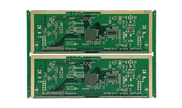
FR-4 PCB design guidelines help engineers achieve reliable performance, stable signal transmission, and efficient manufacturability. By focusing on key design factors, it is possible to optimize both electrical and thermal performance.
Ground Plane
Typically dedicated to an entire layer and placed close to the top layer, providing excellent signal reference and EMI shielding for reliable multilayer PCB board performance.
Power Plane
Located in the middle of the board, the power plane distributes power throughout the circuit, reduces power impedance, and improves electrical stability.
Signal Layers
The remaining layers are used for signal routing. The proper stacking of layers enables optimizing routing density, impedance, and signal integrity.
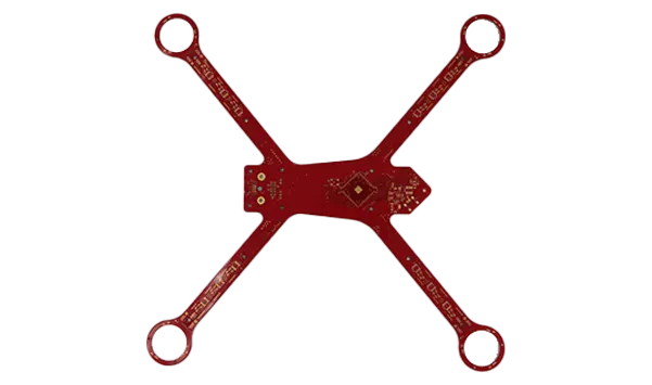
FR-4 PCB design guidelines help engineers achieve reliable performance, stable signal transmission, and efficient manufacturability. By focusing on key design factors, it is possible to optimize both electrical and thermal performance.
Multilayer PCB Stack-Up Design
Stack-up of the Multilayer PCB is very crucial in determining the signal integrity, power distribution, EMI performance, and manufacturability. Good design of the stack-up provides electrical stability, mechanical stability, and repeatability, especially in the case of high-speed and high-density products.
The standard stacking options, such as 4-layer, 6-layer, and 8-layer PCBs, are chosen depending on the complexity of circuits and their performance requirements. Important aspects, including dielectric thickness, copper weight, and layer stacking, need to be taken into consideration to obtain controlled impedance, proper heat dissipation, and crosstalk reduction.
Being a multilayer PCB manufacturer with great experience in this area, Benlida offers valuable advice about optimal layer stacking.
Industries Served by Multilayer PCB Solutions
These boards are used in applications that require high-density routing, compact construction, and defined electrical performance. The required build depends on the application’s electrical, mechanical, thermal, and production conditions.
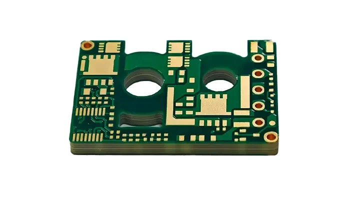
Industrial Control Systems
Employed in programmable logic controllers, automation systems, and control systems in industry.
Guarantees reliable functioning for prolonged use and complicated circuitry demands.
Communication Equipment
Applied in networking devices, communication modules, and signal transmission systems. Supports high-speed signal transmission and high-frequency circuit applications.
Automotive Electronics
Utilized in automotive control systems, intelligent driving systems, and electronic devices used inside vehicles. Satisfies needs for reliability, strength, and dependable functioning amid tough conditions.
Medical Equipment
Employed in medical equipment, monitoring systems, and diagnostic devices. Suitable for applications demanding accuracy and safety, along with reliable performance.
Consumer Electronics
Used in smart devices, electronic products, and compact portable equipment.
Enables miniaturization, higher integration, and improved product performance.
Aerospace Applications
Useful for electronic systems requiring lightweight design, reliability, and environmental protection. Supports complex PCB structures and advanced manufacturing requirements.