

High-Frequency PCB Manufacturing
High-Frequency PCB Manufacturing for RF and Microwave Designs
Benlida provides custom high frequency PCB design and manufacturing solutions for RF, microwave, and high-speed electronic applications. With advanced materials, precise impedance control, and reliable quality management, we support both prototype development and volume production.
RF Laminate & Stack-Up Requirements
Controlled Impedance Targets
Project-Defined Verification Criteria
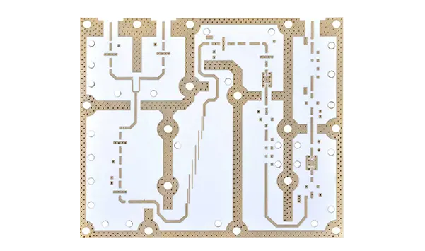
Our High-Frequency PCB Manufacturing Capabilities
At Benlida, we provide advanced high frequency PCB manufacturing capabilities with 2–20+ layer fabrication, precision impedance control, and high-density PCB production expertise. Laser drilling, PTFE surface activation, and sequential lamination are construction-specific options, not default steps. Their availability, processing route, controls, and verification requirements are subject to engineering and quotation review for the exact material grade and stack-up.
For a conventional multilayer build not primarily driven by RF or microwave requirements, review multilayer PCB manufacturing. If laser microvias, build-up structures, or sequential lamination drive the construction, review HDI PCB manufacturing.
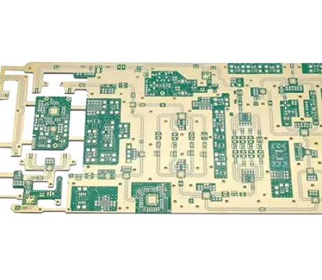
Layer Count
2-20+ layers
Minimum Via Size
0.1 mm
Impedance Control
±5%
PTFE Surface Activation Review
Some PTFE-based laminates may require sodium or plasma activation before hole-wall metallization. The route must follow the supplier guidance for the approved grade and construction, and availability is subject to quotation review.
MOQ
1 pcs
Packaging
ESD protection materials, moisture-barrier bags, bubble wrap, and corrugated cartons.
Minimum Trace/Space
4/4 mil (0.10/0.10 mm)
Thickness Tolerance
±10%
Laser Drilling
High-precision microvias for HDI and RF designs
Hybrid/Sequential Lamination Review
Hybrid constructions require review of the exact laminate and bonding combination, press route, via structure, registration, dimensional behavior, and verification plan. Sequential lamination is not required for every high-frequency PCB; availability is subject to stack-up review.
OEM/ODM
available
Materials for High-Frequency PCBs
Substrate material selection is very crucial for the effectiveness of high frequency PCBs since the dielectric properties and signal loss have direct influences on the effectiveness of signal transmission and stability. Unlike FR-4 substrates that are used in standard PCBs, high frequency PCBs use special substrates such as Rogers and PTFE, which have low dielectric loss, high frequency stability, and consistent electrical performance at all frequencies.
For exact-grade information, read our RO4350B material properties and selection guide. For general glass-reinforced epoxy board requirements, see FR-4 PCB manufacturing. These resources do not confirm material availability for a specific RF build; availability remains subject to exact-grade and stack-up review.
FR-4
Dk
~4.2-4.8
Df
High
Frequency Stability
Poor
Cost Level
Low
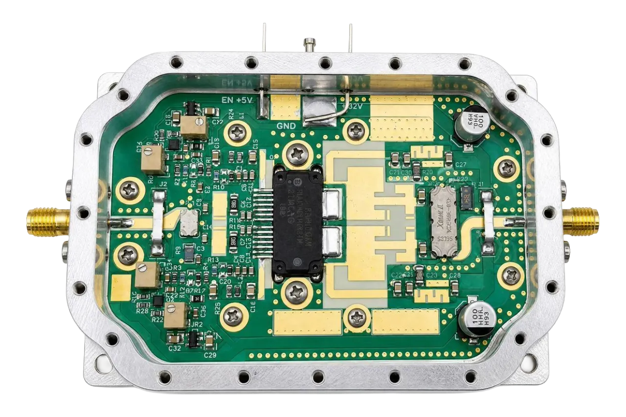
Rogers RO4350B
Dk
~3.48
Df
Low
Frequency Stability
Excellent
Cost Level
Medium
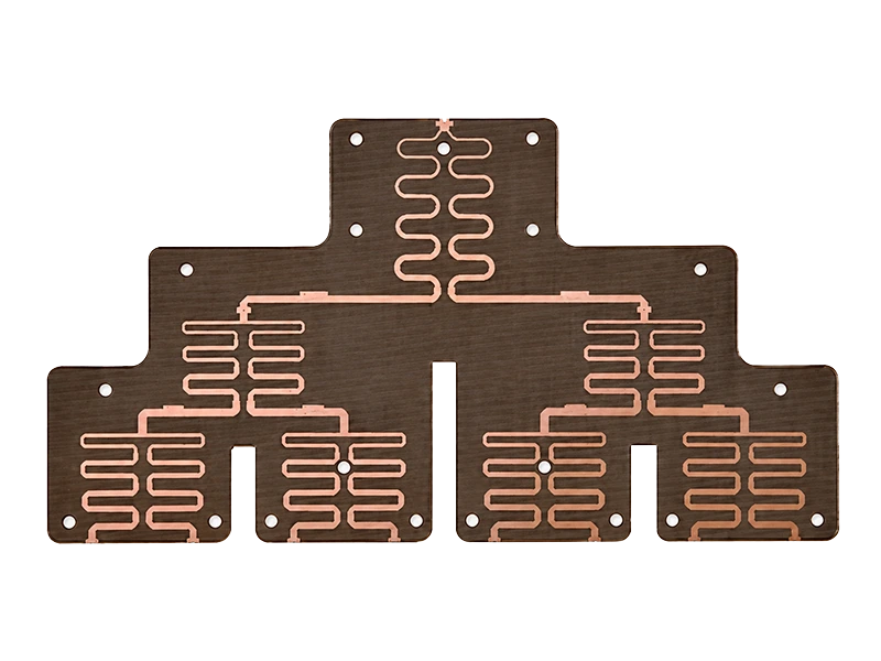
PTFE
Dk
~2.1
Df
Very Low
Frequency Stability
Outstanding
Cost Level
High
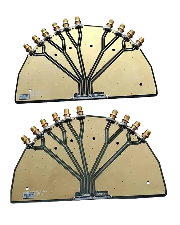
What Is a High-Frequency PCB?
Overview
A PCB becomes a high-frequency design when interconnect behavior must be treated as part of the electrical circuit. There is no universal frequency threshold. Relevant conditions may include RF or microwave operating bands, fast digital edge rates, electrically long traces, controlled transmission lines, low-loss targets, phase requirements, or sensitive launches and via transitions. Material properties, stack-up, finished geometry, copper profile, surface finish, and the agreed verification method must be reviewed together.
RF/microwave and high-speed digital designs overlap, but they are not identical. RF work often emphasizes frequency response, loss, reflection, phase, power, and PIM. High-speed digital work often emphasizes edge rate, channel loss, impedance discontinuities, crosstalk, timing, and eye performance.
Related resources: For routing, return-path, launch, via, and material-selection fundamentals, see our high-frequency PCB design guide. For broader bare-board production options and common manufacturing inputs, review our general bare PCB manufacturing capabilities.
Control the Finished Geometry, Not Only the Nominal Design
RF behavior is affected by the geometry that remains after fabrication. Base copper, plating, finished copper thickness, etch factor, top and bottom conductor widths, sidewall shape, pressed dielectric thickness, the copper-to-dielectric interface, solder-mask condition, via transitions, and residual stubs can affect impedance and loss. The effect depends on frequency, transmission-line structure, field distribution, and the agreed acceptance method.
In the fabrication data, identify critical RF traces and launches, coupon structures, finished-geometry tolerances, the copper foil/profile or roughness used in the electrical model, via definitions, backdrill depth, and maximum residual stub. Smoother copper can help reduce conductor loss at higher frequencies, but a foil trade name or profile label alone does not guarantee a finished-board insertion-loss value.
Mechanically drilled holes, laser microvias, blind/buried vias, and backdrill are different construction choices. Specify the applicable diameter basis—tool, entry/bottom, or finished—together with the layer span, pad and clearance, aspect ratio where relevant, material and stack-up conditions, stub target, tolerance, verification, sampling, and report requirements. Final availability is confirmed only after review of the complete project data.
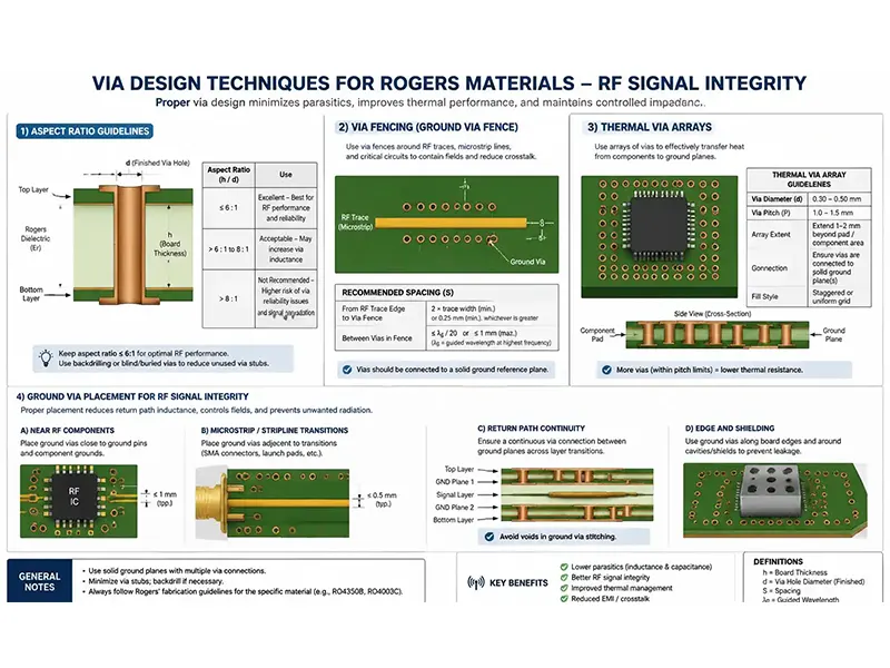
Ground-via fence spacing, placement, connectivity, and electromagnetic purpose remain customer electrical-design inputs. Fabrication review is limited to the manufacturing constraints agreed for the project and does not by itself verify a specified shielding, return-path, crosstalk, or other RF result.
For through-hole, blind, buried, and laser-microvia definitions and basic backdrill terminology, see PCB via types and manufacturing requirements. To define impedance targets, tolerances, coupons, TDR, and report requirements, see how to specify PCB impedance control.
High-Frequency PCB Testing & Inspection
In order to ensure reliable operation in RF, microwave, and high-speed electronics applications, Benlida provides a thorough test and inspection process during the manufacturing of high frequency PCBs. Our quality control system covers electrical performance verification, structural inspection, and functional testing to ensure every high frequency PCB meets strict reliability and performance requirements.
For general inspection, testing, and record scope, see the PCB testing and quality control overview. If the request concerns testing an assembled board against defined functions, see PCBA functional testing. Neither page should be treated as proof of project-specific RF performance.
Electrical Testing
Testing is done in order to check circuit conductivity, insulation resistance, and the possibility of open and short circuit problems. The test ensures proper electrical connection and signal transmission in high frequency PCB applications.
AOI Inspection
The Automated Optical Inspection (AOI) process is done in order to identify any manufacturing defects, such as traces, lines, shorts, and copper layer problems.
X-Ray Inspection
The X-ray inspection provides a way through which a comprehensive evaluation of the internal structure of the PCB can be carried out through quality assurance and the integrity of multi-layer boards. This is crucial for high-frequency circuit board designs where the accuracy and reliability of the internal layers should be taken into account.
Impedance Testing
Impedance control ensures proper functioning of a signal on high frequency PCBs. Impedance testing is used by Benlida to guarantee that a signal passes through a trace according to the design requirements.
Functional Testing
Functional testing evaluates the overall performance and reliability of finished PCBs under actual operating conditions. This final verification step helps ensure that each high frequency PCB delivers consistent performance before shipment.
High-Frequency PCB Manufacturing Process
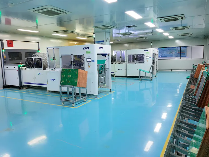
At Benlida, our high frequency PCB manufacturing process covers the complete production workflow from PCB design and DFM review to fabrication, testing, and final delivery. Thanks to precision process control in all the stages of production, including material preparation, multilayer lamination, drilling, plating, and inspection, we provide reliability and quality of the products in high-frequency applications.
1
Material Selection & Engineering Review
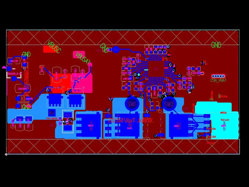
Our engineers evaluate design requirements and select suitable high-frequency materials based on dielectric constant (Dk), dissipation factor (Df), signal speed, and application requirements.
2
High-Frequency Stack-Up Design
The PCB layer structure is carefully designed to control impedance, minimize signal loss, and maintain stable electrical performance for RF and high-speed applications.
3
Inner-Layer Imaging, Etching, and Geometry Control
Inner-layer circuits are imaged and etched according to the approved production data. Process control focuses on material-specific dimensional behavior, base copper, etch compensation, and the resulting conductor geometry. Critical finished trace/space and inspection requirements are applied according to the fabrication documentation.
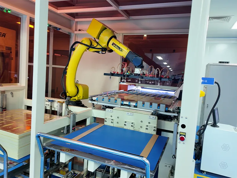
4
Material-Specific Lamination and Dimensional Control
Cores, bonding materials, and copper layers are aligned and laminated using the approved material-specific press route. Process control covers layer registration, pressed dielectric thickness, resin flow where applicable, and dimensional behavior. The completed construction is reviewed against the approved stack-up and applicable acceptance requirements before subsequent processing.
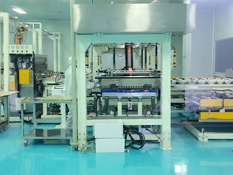
5
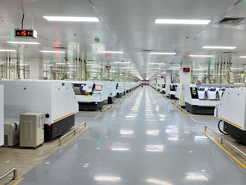
Precision Drilling & Via Processing
High-accuracy drilling creates through holes and vias while minimizing mechanical impact on specialized high-frequency materials.
6
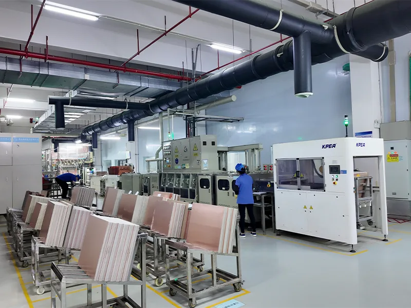
Copper Plating & Circuit Enhancement
Copper plating strengthens electrical connections and ensures stable conductivity across PCB layers for long-term high-frequency signal transmission.
7
Surface Finishing & Performance Protection
Suitable surface finishes and protective coatings are applied to maintain solderability while reducing potential effects on high-frequency performance.
8
Electrical Testing & Signal Verification
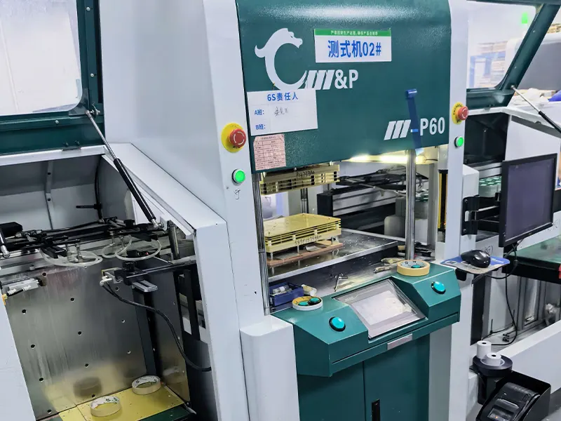
High-frequency PCBs undergo impedance testing, electrical inspection, and quality verification to ensure signal reliability and compliance with design specifications.
High-Frequency PCB Surface Finishes
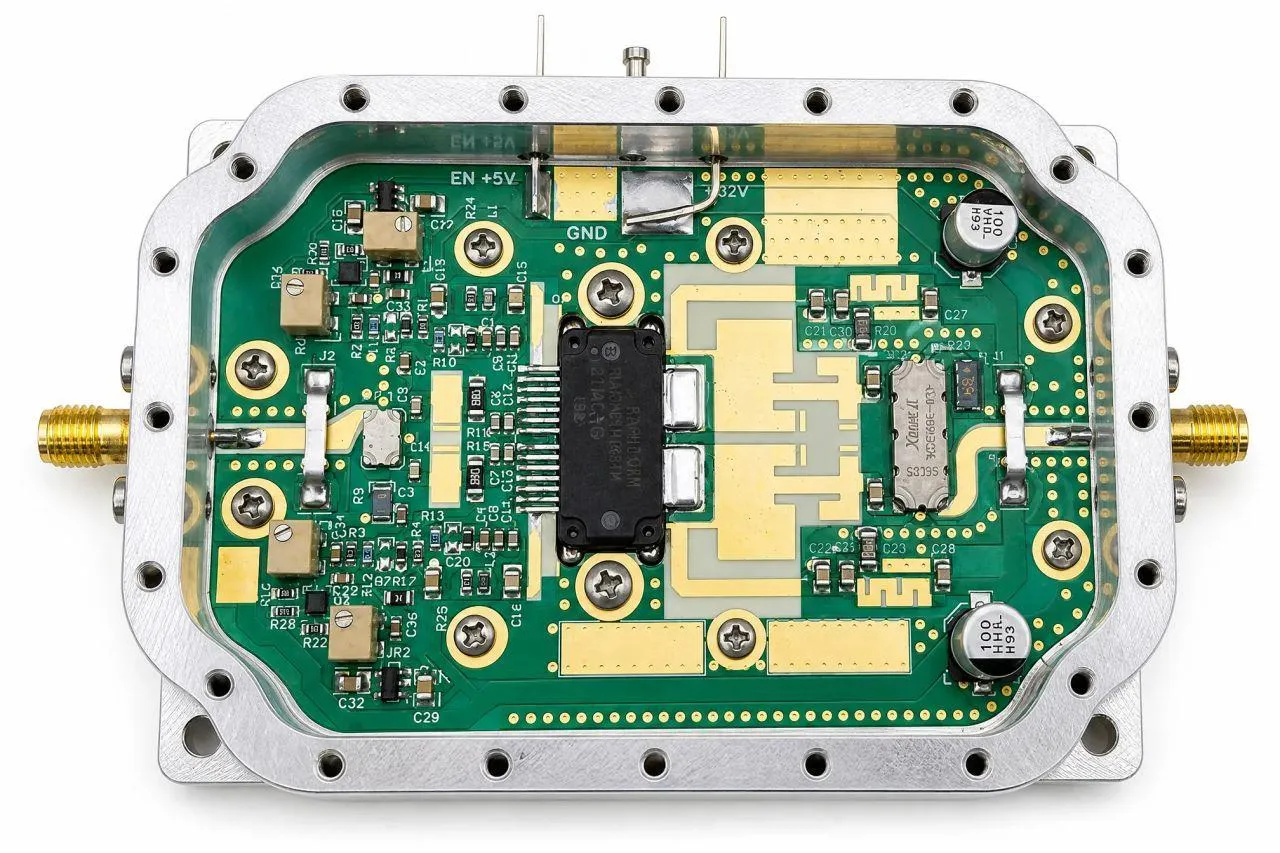
At Benlida, there are many high frequency PCB surface finish types available, like HASL, Lead-Free HASL, ENIG, Immersion Tin, Immersion Silver, and OSP, to cater to various needs. Selection of surface finishes ensures solderability, reliability of the surface, and stability for use in high frequency PCB applications.
For a broader comparison of finish options across process, assembly, storage, reliability, and RF conditions, review the PCB surface finish comparison. Final selection remains project-specific.
HASL
A traditional, cost-effective finish using molten solder, ideal for general-purpose PCBs.
Lead-Free HASL
Environmentally friendly version of HASL, meeting RoHS standards for lead-free electronics.
ENIG
Provides a flat, gold-coated surface for excellent solderability and reliable high-frequency performance.
Immersion Tin
Offers uniform, smooth surface with good solderability for short to medium-term applications.
Immersion Silver
Provides high conductivity and excellent surface planarity for precision assembly and fine-pitch parts.
OSP
Organic solderability preservative protects copper while remaining flat, perfect for fine-pitch components.
High-Frequency PCB Applications
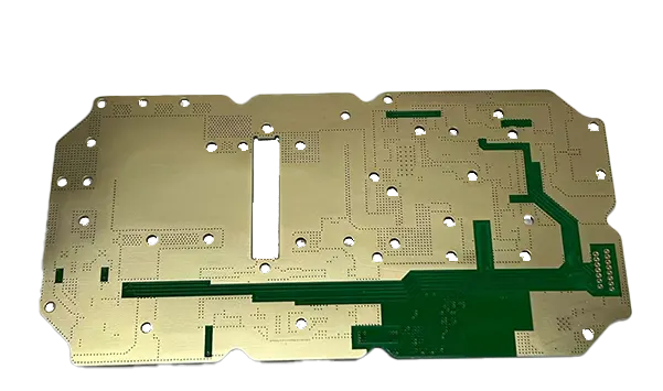
High frequency PCBs are widely used in industries that require reliable signal transmission, low signal loss, and excellent electrical performance. With advanced material options, precise impedance control, and optimized high frequency PCB design, Benlida provides reliable PCB solutions for RF, microwave, and high-speed electronic applications.
Communication Systems
High frequency PCBs have their application in wireless communication systems, 5G systems, base stations, and high-speed data transmission equipment. With their low-loss features and stability in signal transmission, their efficiency in communication increases.
Radar Systems
Radar systems require precise signal transmission and excellent signal integrity to achieve accurate detection and measurement. High frequency PCB solutions provide controlled impedance, stable electrical performance, and reliable operation for advanced radar applications.
Satellite & Aerospace
Satellite and aerospace electronics demand highly reliable PCB solutions that can perform under complex operating conditions. High frequency PCBs are widely used in satellite communication systems, navigation equipment, and aerospace electronics due to their superior electrical stability and durability.
Automotive Electronics
With the development of intelligent vehicles and autonomous driving technologies, high frequency PCBs are increasingly used in automotive radar systems, ADAS, and high-speed control modules. Reliable high frequency PCB manufacturing helps ensure stable data transmission and consistent performance in automotive applications.
Medical Electronics
Advanced medical equipment often requires precise signal processing and reliable electronic performance. High frequency PCBs support high-performance medical devices and testing systems by providing stable signal transmission and excellent electrical characteristics.
Industrial & High-Speed Electronics
High frequency PCB solutions are also applied in industrial automation, control systems, and advanced electronic equipment. Through professional high frequency PCB design and manufacturing processes, these applications can achieve improved signal integrity and system reliability.
Why Choose Benlida for High-Frequency PCB Manufacturing?
Experienced High Frequency PCB Manufacturer
Benlida is an experienced high frequency PCB manufacturer specializing in reliable PCB solutions for RF, microwave, and high-speed electronic applications. With extensive experience in professional PCB manufacturing and full production capability, we can help customers from PCB design and prototyping to mass production.
Advanced Manufacturing Capabilities
High-frequency PCB projects require review against the approved material grade and stack-up. Laser microvias, PTFE surface activation, and sequential lamination are construction-specific options, not default steps. Availability, processing route, controls, and verification requirements are subject to project review before production.
Strict Quality Control
To ensure the reliability of all high frequency PCBs, Benlida uses thorough quality control through each step of the manufacturing process. With advanced inspections like AOI, X-ray, and electrical tests, we can ensure the quality of our products in a tough high-frequency environment.
Flexible Custom Production
As an experienced high frequency PCB manufacturer,Benlida provides flexible manufacturing solutions from prototype quantities to mass production, with OEM/ODM services available. Our customized high frequency PCB manufacturing capabilities allow us to meet different project requirements with consistent quality and reliable delivery.
High-Frequency PCB Design Guides
Benlida High Frequency PCB Design Solutions: Engineered for Precision, Signal Integrity, and High-Performance Applications.
The process of designing an effective high frequency PCB involves accurate control of impedance, signal integrity, electromagnetic interference, and trace layout.
Benlida offers expert guidance on how to design a good high-frequency PCB solution with stable signal transmission through proper manufacturing. Proper selection of stack-up structure and materials, along with routing, makes the PCB perform consistently in high-speed and RF applications.

Effective design focuses on controlling impedance, minimizing electromagnetic interference, and optimizing trace layouts.
Avoid Sharp Corners (Use Curved Traces)
In the process of designing high frequency PCBs, sharp traces might create impedance mismatches and reflections of the signal. The use of curved traces will guarantee that there will be smooth signal flow, which improves signal performance.
Minimize Signal Loss and Reflections
High frequency signals are very susceptible to losses and reflections of the signal, which could lead to degradation of the overall performance of the PCB. Appropriate techniques for high frequency PCB designs, such as proper trace routing, material choice, and dielectric control, are useful in minimizing energy losses.
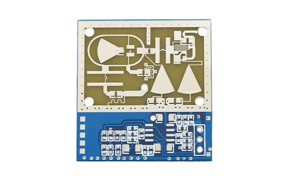
High Frequency PCB design guidelines help engineers achieve reliable performance, stable signal transmission, and efficient manufacturability.
Maintain Consistent Impedance
One of the main prerequisites of high frequency PCB design in the case of RF and microwave applications is the ability to maintain constant impedance. Controlled stack-up, trace size, and proper materials selection can avoid signal degradation.
Short Signal Paths for RF Signals
Short trace paths are very important for the efficient operation of RF signals. The use of short traces in high frequency PCB layout is necessary in order to avoid signal delay, transmission loss, and electromagnetic interference.
High Frequency PCB Design Considerations
When developing a high frequency PCB design, engineers should consider several key factors, including material selection, layer stack-up, impedance control, and signal routing. Proper design planning helps reduce signal loss, minimize interference, and ensure reliable performance in demanding RF, microwave, and high-speed applications.
Characteristics of High-Frequency PCBs
High frequency PCBs are meant to ensure signal transmission stability and effective electrical performance in RF, microwave, and high-speed electronic devices. Using special materials, optimized structure design, and precision in the production process, high frequency PCBs offer high integrity and consistency of signals as well as low transmission losses at high frequencies.
Low Signal Loss
High frequency PCBs employ low-loss materials and optimized structures to reduce the amount of energy loss in the signal transmission process.
Excellent Signal Integrity
It is important to preserve signal integrity for high-frequency designs. The right choice of materials, proper impedance, and proper design of high frequency PCBs will help minimize signal distortion, reflections, and electromagnetic interference.
Precise Impedance Control
Impedance control plays an important role in the proper operation of high-frequency PCBs. The advanced process of manufacturing allows the designers to manage the width of the traces, the thickness of dielectrics, and the stack-up structure of the PCB.
Superior Frequency Stability
The high-frequency PCBs employ specific laminates, which have stable dielectric properties and low dissipation factors, unlike FR-4 PCBs.
High Reliability Performance
Through advanced high frequency PCB manufacturing processes and strict quality control, high frequency PCBs provide reliable performance for demanding applications such as communication systems, radar, satellite equipment, and automotive electronics.
FAQ
A high-frequency PCB is a board whose interconnects must be treated as part of the electrical circuit. There is no universal frequency cutoff. Operating band, edge rate, path length, transmission-line structure, material properties, stack-up, copper, vias, launches, surface finish, and verification method can all matter. RF/microwave and high-speed digital requirements can overlap, but they should be reviewed against their own electrical targets.
Availability is confirmed by the exact manufacturer, grade, construction, thickness, copper, quantity, and current supply status. “Rogers,” “PTFE,” and “low-loss FR-4” are broad labels, not complete specifications. Identify the required grade and any approved alternatives in the RFQ. The quotation must confirm the procurement and processing route before the material is treated as available. Any proposed substitution requires customer approval before release.
No. Rogers describes RO4350B as a woven-glass-reinforced hydrocarbon/ceramic thermoset laminate in the RO4000 family. It is not PTFE. This distinction matters because PTFE-based laminates may need different drilling, activation, bonding, and dimensional-control processes. Use the exact supplier processing guide for the approved material and stack-up.
Provide the proposed stack-up, exact material and copper requirements, target impedance and tolerance, affected layer and net or controlled structure, transmission-line type, finished line width and spacing, reference plane, solder-mask condition, and coupon or test requirement. Include the Dk source and value type used in the electrical model. Any proposed manufacturing adjustment to critical geometry or material must be documented and approved before release.
No. TDR can verify characteristic impedance or locate impedance discontinuities on an agreed coupon or structure. It does not by itself prove insertion loss, return loss, phase response, PIM, connector behavior, or end-system operation. Those requirements need separately defined test vehicles, fixtures, calibration planes, frequency or power conditions, de-embedding rules, sampling, reports, and acceptance limits. TDR availability and method are confirmed in the quotation.
Bare-board electrical testing checks network continuity and isolation under the agreed method. It can detect opens and shorts, but it does not prove controlled impedance, insertion loss, S-parameters, PIM, assembly quality, or product function. State the required test level, limits, coverage, and report needs in the purchase data. Functional testing belongs to a separately defined PCBA scope.
Confirmation is project-specific and follows engineering review of the exact material grade and construction. PTFE is a broad family, and hybrid builds add bonding, CTE, resin-flow, registration, and pressed-thickness risks. Include the complete stack-up, supplier material designations, copper, via plan, dimensions, and verification requirements in the project data. The quotation should state the approved processing route and any construction limits; an unreviewed combination is not treated as available.
There is no universal best finish. Selection depends on transmission-line field distribution, frequency, loss or PIM sensitivity, solderability, planarity, wire-bond or contact needs, assembly, storage, reliability, availability, and cost. Nickel-bearing ENIG can add loss in some RF structures, but it is not universally unsuitable. Define the critical RF areas and acceptance requirements before the finish is approved.
Prepare the current Gerber or ODB++, NC Drill data, fabrication drawing, proposed stack-up, exact material and copper requirements, surface finish, quantity, target date, and revision. Add the operating band, impedance table, transmission-line structures, critical geometry, via or backdrill requirements, electrical and coupon/test requirements, approved alternatives, traceability and material-documentation requirements, and required inspection/test reports. If PCBA is requested, also prepare the BOM, centroid data, assembly drawings, and test or programming requirements. Use an approved transfer channel for manufacturing files.
MOQ and lead time are confirmed for each project and should not be inferred from a generic page. They depend on material availability, exact grade and thickness, stack-up, tooling, lamination cycles, via structure, finish, inspection/test scope, documentation, quantity, and production loading. A complete project package is required for quotation and schedule review. Prototype and expedited options, if available, must be confirmed in the quotation.
Prepare Your High-Frequency PCB RFQ
Share the latest board revision and the requirements already defined. Mark each requirement as mandatory, preferred, or open to review. If some information is not ready, state the design stage and the decisions still open.
Core Board & Order Details
- Current Gerber or ODB++ manufacturing data, drill data and definitions—including NC Drill files where needed—and a dimensioned fabrication drawing. Identify the board name and revision.
- Layer count, finished board thickness, base and finished copper requirements, solder mask, legend, and surface finish.
- Exact laminate, core, bondply, or prepreg grades where defined. State whether alternatives may be proposed and who approves changes.
- Special process requirements, quantity by revision, delivery destination, target date, and applicable fabrication and acceptance requirements.
RF, Stack-Up & Verification Requirements
Include the following where they affect the design or acceptance requirements:
- Operating band or digital edge/channel requirements, proposed stack-up, and pressed dielectric thickness targets.
- Impedance targets and tolerances, with the relevant layers, nets, and transmission-line structures.
- Specified Dk source and value type, copper profile or roughness, and critical finished conductor dimensions and tolerances.
- Via, backdrill, and residual-stub requirements. For ground-via fences, define spacing, placement, layer connections, and electrical intent.
- Required coupons, TDR method, sampling, and reports. For insertion-loss, return-loss, phase, S-parameter, or PIM requirements, identify the test structure, test conditions, and acceptance limits.
Ground-via fence geometry and electrical intent are customer design inputs. A manufacturability review does not, by itself, validate shielding, return paths, crosstalk, or RF performance.
Supporting Files & Delivery Requirements
- If available and agreed for review: native CAD or controlled stack-up files, a netlist or agreed intelligent data, and assembly keep-outs that affect bare-board fabrication.
- If available: a previous approved stack-up or anonymized measurements relevant to the current revision.
- State any required packaging, material lot traceability, material documents, inspection/test reports, or record-retention terms.
- Add forecast quantities and revision-transition requirements where relevant.
PCBA Additions — Only If Assembly Is Requested
If the project also requires component sourcing, SMT/THT assembly, programming, or assembly-level testing, review PCB assembly services before preparing the additional PCBA package.
- BOM, centroid/pick-and-place data, and assembly drawings.
- Component sourcing scope and approved substitution rules.
- Programming data, test procedure, fixture information, acceptance criteria, and assembled quantity, where applicable.
These PCBA files are additional to the bare-board package. Requested materials, special processes, and verification methods are subject to project review and quotation confirmation. Listing a requirement here does not confirm its availability.
Discuss Your High-Frequency PCB Requirements
Share the current board revision, proposed stack-up, exact material requirements, impedance targets, quantity, target date, and required verification. These inputs support manufacturability and quotation review for the proposed construction. Material availability, special processes, test scope, and quotation terms are confirmed for each project.