

DIP PCB Assembly Services
Through-Hole Assembly for Prototype and Production Projects
Discuss your DIP and other through-hole component requirements with Benlida. Send your BOM, assembly drawing, board information, planned quantity, and design revision for review.
For mixed-technology designs, identify both SMT and through-hole components. Include your sourcing model and any inspection or functional testing requirements. Assembly methods, test scope, and delivery terms are confirmed for each project.
For an overview of assembly routes, sourcing models, testing, and RFQ inputs, see our PCB assembly services.
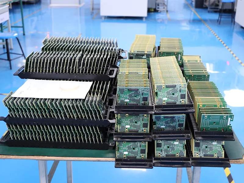
Through-Hole Components and Project Types
DIP packages are one group of through-hole components. Other projects may include leaded resistors and capacitors, connectors, relays, and power components. Part numbers, lead geometry, mounting arrangements, and soldering requirements help determine the assembly route.
For a prototype, explain what the build needs to verify. For a repeat or production order, identify the approved revision, material availability, and planned batch quantity. Tell us whether the board is entirely through-hole or combines SMT and through-hole components.
Prototype DIP Assembly
Provide the design revision, quantity, and validation goals. Identify unusual components and any tests needed for the prototype. Feasibility and the available production route are reviewed before the build is confirmed.
Small-Batch Through-Hole Assembly
Outline the planned batch size and any repeat orders. Component availability, manual work, tooling, and inspection requirements help define the project scope and quotation.
Production Through-Hole Assembly
Production planning requires a released design, an agreed sourcing model, and confirmed material readiness. Insertion methods, soldering, tooling, inspection, and scheduling depend on the assembly. Automated soldering does not mean every component is automatically inserted.
Mixed SMT and Through-Hole Assembly
Identify the components on both sides of the board. The route must account for solder access, component clearances, thermal exposure, and inspection needs. See our SMT assembly services for the surface-mount part of the project.
Inspection and Project-Defined Testing
Inspection and testing are agreed for each project. Specify coverage, test access, fixtures, procedures, operating conditions, and pass/fail limits. Functional testing is a separate scope and should not be assumed to be included in every assembly order.
DIP Packaging and Through-Hole Assembly
DIP stands for dual in-line package. A DIP package has two parallel rows of leads. Through-hole assembly, also called THT assembly, is the broader category for components mounted through holes in a PCB. It includes DIP packages and other leaded components.
A DIP circuit board uses this structure to provide strong mechanical connections and reliable electrical performance. It is widely used in industrial control systems, power electronics, communication devices, and other products requiring high durability.
How Does Through-Hole Assembly Work?
- Component insertion: Position the specified components using the approved assembly drawing.
- Soldering: Select wave, selective, or hand soldering according to the component and board design.
A professional DIP PCB assembly process helps achieve accurate placement, strong solder joints, and consistent product quality.
Advantages of DIP Technology
- Strong mechanical stability
- Good heat resistance
- Easy maintenance and repair
- Suitable for prototype and mass production
What Determines Assembly Suitability?
- Component ratings and lead geometry
- Finished-hole dimensions and board construction
- Mechanical support and access for service
- Soldering conditions and required verification
If electronic products require long-term, stable operation and high durability, DIP remains a reliable assembly choice.
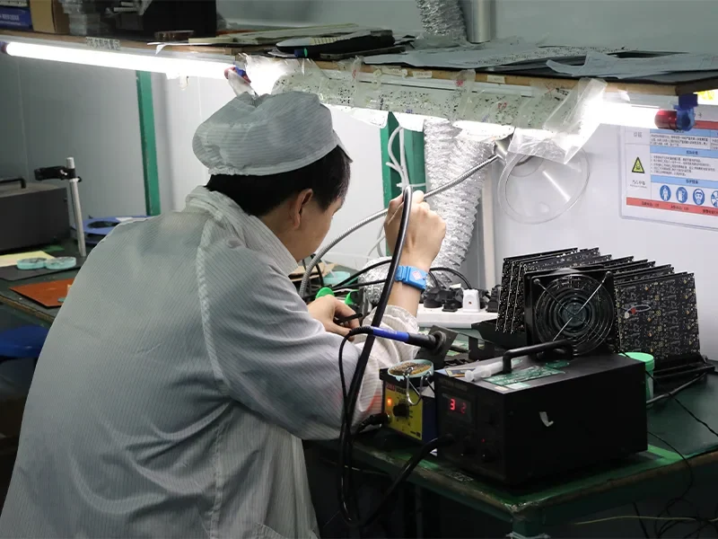
DIP Manufacturing Process Overview
Complete DIP PCB Assembly Process for Reliable Production
A high-quality DIP PCB assembly process requires precise engineering control from design review to final inspection. Benlida follows a structured manufacturing workflow to ensure each DIP circuit board achieves stable performance and long service life.
Design and Revision Review
Review the BOM, assembly drawing, board data, component information, and test requirements. Confirm part numbers, polarity, lead-to-hole fit, clearances, and the current revision. DFM and DFA review do not replace circuit or product validation.
Board and Component Readiness
Agree who supplies the bare PCBs and each group of components. Confirm part identification, quantity, packaging, and the released specification. Proposed substitutions and material changes require approval before use.
Preparation and Insertion
Confirm component orientation, Pin 1, lead alignment, mounting height, and any mechanical support using the released assembly information. Lead forming, retention, and trimming need component-specific instructions and an approved process.
Selected Soldering Route
Choose the soldering method after reviewing the board, component mix, solder access, materials, and quantity. Account for flux application, thermal exposure, tooling, and nearby components.
Inspection and Agreed Testing
Define the inspection coverage, acceptance criteria, and records. Electrical testing, functional testing, and firmware programming are separate activities requiring suitable inputs and an agreed scope.
Release, Labeling, and Packaging
Confirm cleaning or residue handling according to the materials and component requirements. Authorized rework needs reinspection and any necessary retesting. Agree identification, packaging, lead protection, and shipment requirements before release.
Request a Quote for Through-Hole Assembly
For an initial discussion, share your planned quantity, target timing, and a short project description. Tell us which files are available and which details still need review.
For a detailed quotation, provide your BOM, assembly drawing, board information, revision, sourcing model, and inspection or testing requirements. For mixed assembly, include Pick-and-Place/Centroid data when available. Identify unusual leads, heavy components, dense bottom-side layouts, or special cleaning requirements.
Before sharing confidential design information, confirm the file-transfer route and any confidentiality requirements with your contact.
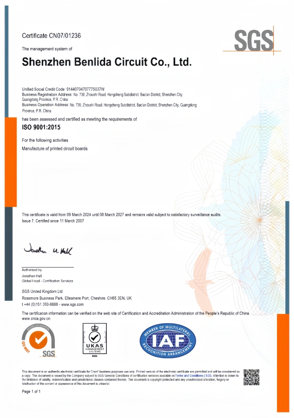
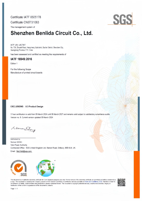
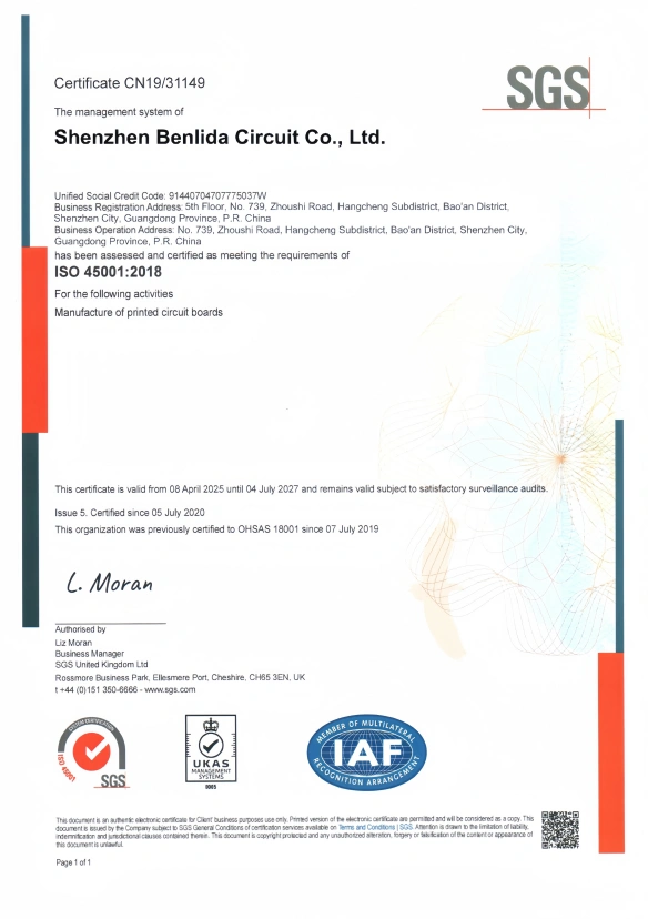
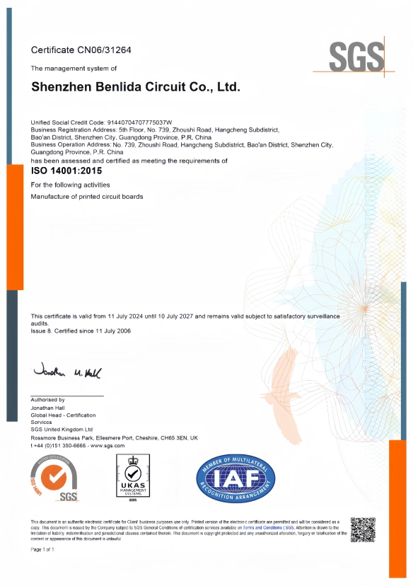
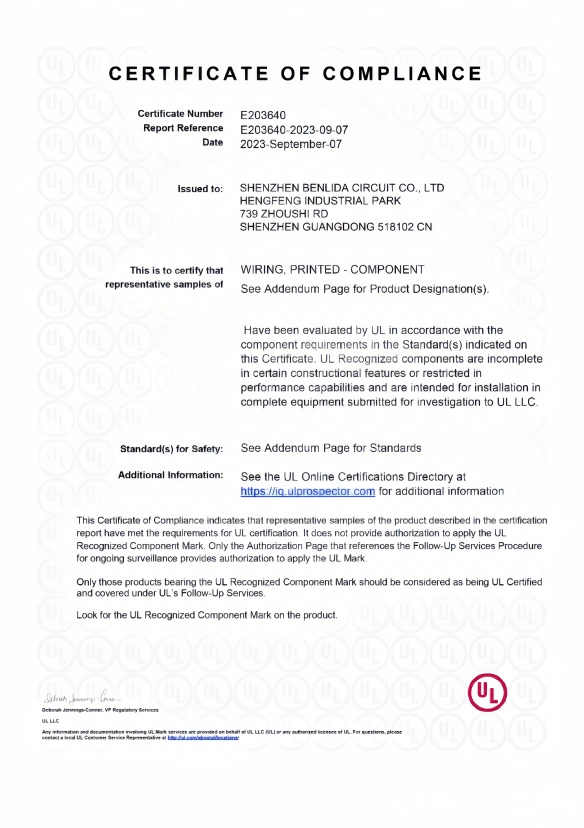
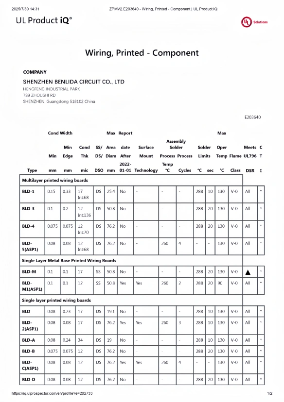
Our Certificates
Certified Quality Standards for Reliable DIP Manufacturing
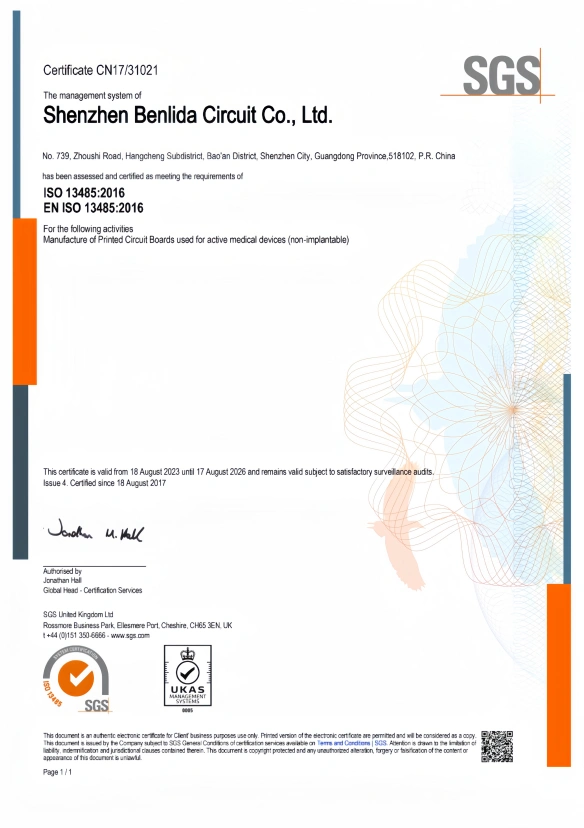
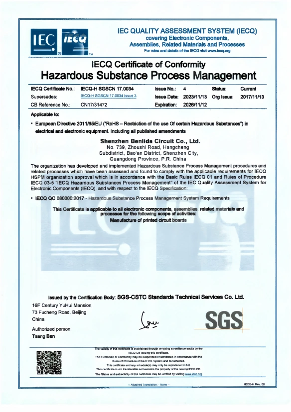
Benlida maintains strict quality management throughout the DIP manufacturing process. Our certifications demonstrate our commitment to production reliability, environmental responsibility, and international manufacturing standards.
With professional PCB manufacturing experience since 2011, we follow standardized processes to ensure every DIP circuit board and assembly project meets customer expectations.
Our certifications include:
- SGS certification
- ISO-related quality management standards
- RoHS compliance
These certifications support reliable DIP PCB assembly production for industries requiring stable and safe electronic solutions.
DIP Assembly Testing & Quality Control
Comprehensive Inspection for Stable Circuit Performance
Quality control is an essential part of every DIP PCB assembly project. Through advanced testing equipment and strict inspection procedures, potential defects can be identified during different production stages.
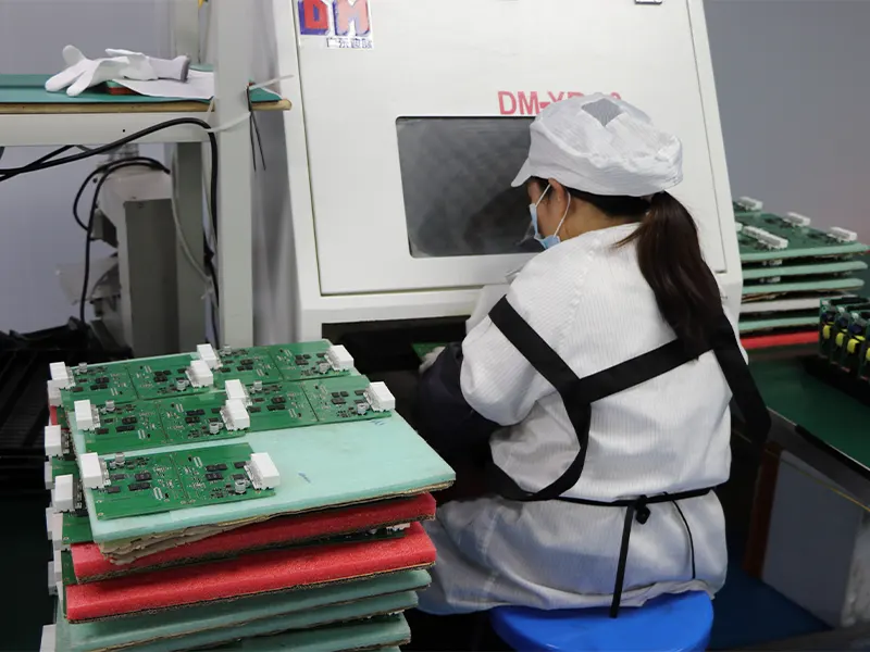
AOI Inspection
Where suitable and specified, automated optical inspection can assess accessible component placement, polarity, and solder features. Component height and obstructions may limit coverage.
X-Ray Inspection
Where appropriate, X-ray inspection can help assess selected joint features that optical inspection cannot see. Define the method, image quality, coverage, and acceptance criteria for the structure being examined.
Electrical Testing
Assembly electrical testing is separate from bare-board electrical testing. Agree the checks, accessible test points, equipment, and pass/fail limits.
Functional Testing
Functional testing checks the functions and operating conditions stated in the agreed test plan. Define the fixture, approved software or firmware, power and load conditions, interfaces, and pass/fail limits. Review functional testing requirements and any firmware programming requirements.
Visual Inspection and Records
Visual inspection can check accessible solder appearance, component condition, orientation, and the PCB surface. Agree the acceptance criteria and records, including any reinspection or retesting after authorized rework.
Define Your Through-Hole Assembly Project
Discuss the decisions that affect feasibility, cost, and acceptance with Benlida. Confirm the build scope before committing to production.
Component and Design Review
Share the component part numbers, board data, and assembly drawing. Raise questions about lead fit, orientation, mounting, and access before the design is released.
Soldering Route
Discuss the component mix, board construction, and soldering access. Confirm the proposed process and any tooling or special handling before production commitments are made.
Production Planning
State prototype and production quantities separately. Material readiness, tooling, approved revisions, and inspection or test requirements affect the schedule.
Inspection and Test Scope
Confirm the checks and records required for the project. Agree which inspection and test methods the order includes, along with coverage and acceptance criteria.
Component Supply
Identify customer-supplied and sourced parts. Confirm availability, approved alternatives, and material responsibilities before the affected work is released.
Applications and Design Conditions
Where Are DIP PCB Assembly Solutions Used?
With excellent mechanical strength and long-term reliability, DIP PCB assembly remains widely used in industries that require stable operation.
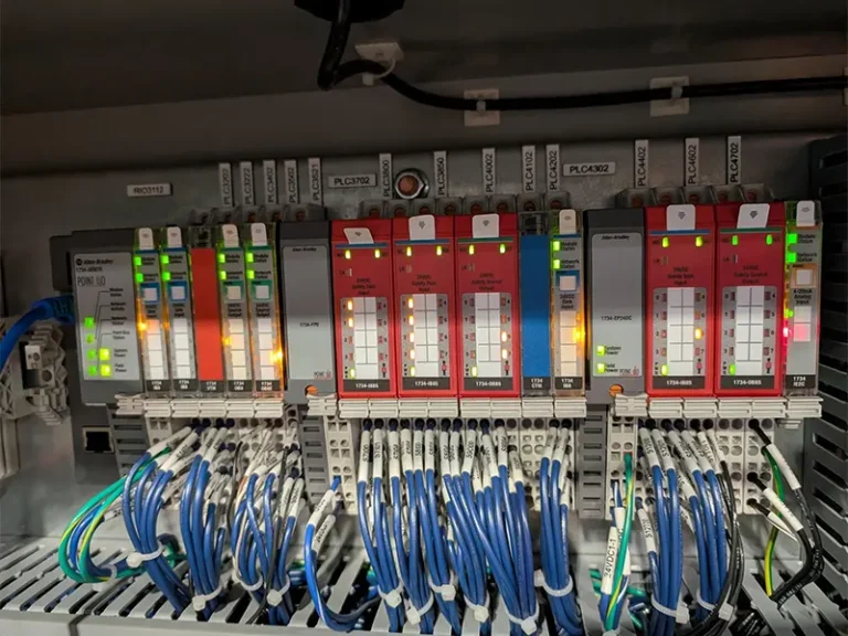
Industrial Control Equipment
Industrial equipment often operates under demanding conditions requiring durable electronic connections.
A DIP circuit board is commonly applied in:
A DIP circuit board is commonly applied in:
- PLC control systems
- Automation equipment
- Industrial controllers
- Monitoring systems
The strong solder connection of DIP components helps improve reliability in continuous operation environments.
For controllers, monitoring systems, and automation equipment, identify connectors, relays, service access, and the operating environment. State any vibration or mechanical support requirements.
1
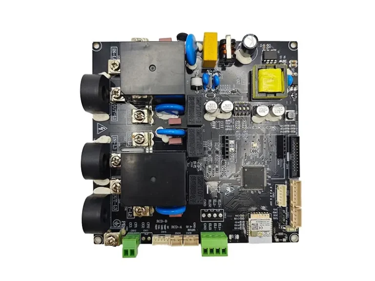
Power Electronics
Power-related applications usually require components with better heat resistance and mechanical stability.
DIP assembly is suitable for:
- Power supply units
- Inverters
- Charging equipment
- Energy management systems
The through-hole structure provides strong support for larger components.
For power supplies, inverters, and charging equipment, identify large terminals, heavy components, copper distribution, and thermal constraints. Mechanical retention and soldering access need design review.
2
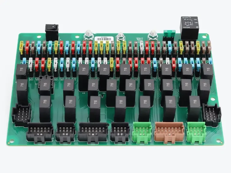
Automotive Electronics
Automotive systems require electronic products that can withstand vibration and temperature changes.
DIP technology is used in:
- Vehicle control modules
- Electronic control systems
- Sensor devices
- Power management equipment
Reliable DIP circuit board manufacturing helps improve product durability.
Provide the operating conditions, component specifications, traceability requirements, and acceptance plan. Specify how vibration, temperature exposure, and durability will be evaluated for the finished product.
3
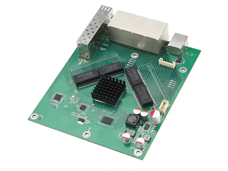
Communication Equipment
Communication devices require stable signal transmission and long service life.
DIP solutions can support:
- Network devices
- Signal processing equipment
- Communication control systems
For network and communication assemblies, describe connectors, shielding, interfaces, and inspection or test access. Define the functions and conditions that need verification.
4
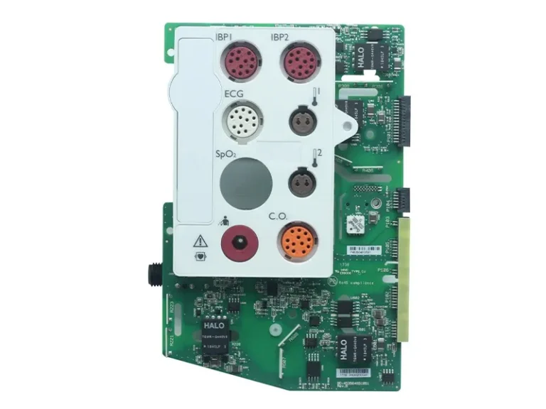
Medical and Industrial Instruments
Many medical and testing devices require dependable electronic performance.
A professional DIP PCB assembly process helps ensure accurate operation and long-term stability for precision equipment.
Provide the assembly specification, handling requirements, test procedures, and acceptance criteria for the instrument. Define how measurement accuracy and stability will be verified under the intended operating conditions.
5
Choosing a Through-Hole Soldering Process
Flexible DIP Manufacturing Methods for Different Requirements
Different products require different soldering approaches. Benlida provides multiple DIP assembly methods according to PCB design, production volume, and application requirements.
The component mix and board layout help determine the soldering route. Review the three methods below with the project team. Confirm solder alloy requirements separately.
Wave Soldering
Automatic wave soldering is one of the most common methods used in high-volume DIP PCB assembly production.
• High production efficiency
• Consistent solder quality
• Suitable for large quantities
• Reduced manual operation
During the process, assembled PCB boards pass through a controlled solder wave that creates strong connections between component pins and PCB pads.
This method is ideal for products requiring stable and continuous manufacturing.
Wave soldering may suit assemblies with accessible through-hole joints and a compatible layout. Review underside components, thermal exposure, flux and alloy requirements, board support, and any pallet or masking needs. Production quantity is one input to process selection.
Selective Soldering
Selective soldering provides higher flexibility for complex PCB designs.
• Precise soldering position control
• Suitable for mixed SMT and DIP boards
• Reduced thermal impact
• Better protection for sensitive components
For advanced DIP circuit board applications, selective soldering helps achieve reliable connections in areas where traditional wave soldering may not be suitable.
Selective soldering targets defined joint locations. Review nozzle access, lead length, nearby components, board position, and thermal requirements. Tooling and programming depend on the equipment configuration and assembly design.
Hand Soldering
Manual soldering remains valuable for prototypes, customized products, and special components.
• Prototype production
• Low-volume manufacturing
• Repair projects
• Special component assembly
Experienced technicians can handle unique designs and provide additional flexibility for customized DIP PCB assembly requirements.
Controlled hand soldering may be considered for particular components, limited quantities, or joints needing a different approach. It requires suitable tools, handling controls, process instructions, and inspection. Production soldering, authorized rework, and repair are different scopes.
Solder Alloy Requirements — Separate from Method Selection
Environmental requirements are becoming increasingly important in electronic manufacturing. RoHS-compliant processes help ensure that DIP circuit board products meet international standards.
Lead-free DIP assembly provides:
• Compliance with environmental regulations
• Reduced harmful material usage
• Reliable solder performance
• Support for global market requirements
Lead-free is a solder alloy requirement, not a fourth soldering method. Specify the required alloy and any component or board-finish restrictions. Confirm compatibility with the proposed soldering and rework process before production.
DIP Assembly Core Capability Parameters
Advanced Manufacturing Capability Supporting Reliable Production
Benlida provides professional DIP manufacturing capabilities with flexible production options. The following parameters demonstrate our ability to support different DIP PCB assembly requirements.
These capabilities allow Benlida to provide dependable DIP circuit board solutions for various electronic manufacturing needs.
Through-Hole Assembly FAQs
DIP is a dual in-line package with two parallel rows of leads. Through-hole assembly is the broader process used for components mounted through PCB holes. SMT mounts components on surface pads. A mixed assembly can use both SMT and through-hole components.
Through-hole components may be used in industrial controls, power electronics, communication equipment, automotive electronics, and instruments. Suitability depends on the component, board design, operating conditions, and required verification. Share the actual application requirements for review.
Through-hole assembly can be used for production builds, but the route and schedule depend on the design, component supply, insertion work, soldering access, tooling, and agreed testing. Confirm the accepted batch quantity and route with Benlida. Automatic insertion should not be assumed from the use of automated soldering.
For an initial discussion, provide the quantity, target timing, and a project summary. A detailed quotation normally needs the BOM, assembly drawing, board information, revision, sourcing model, and inspection or test requirements. If bare PCB fabrication is included, provide the fabrication data. Include Pick-and-Place/Centroid data for mixed assembly when available.
State which boards and parts you plan to supply and which you want Benlida to source. Confirm the accepted supply model, identification, quantity, packaging, material readiness, and responsibility for shortages before the build. Alternatives require approval before use.
Yes, a board can combine both technologies. Identify the SMT and through-hole parts on both sides of the board. Review the process sequence, solder access, component clearances, thermal restrictions, and inspection requirements before confirming the build.
Visual inspection, AOI, X-ray inspection, electrical testing, and functional testing serve different purposes. The applicable methods, coverage, inputs, limits, and records are agreed for the project. Functional testing is not automatically included in every order; confirm its scope and any fixture or software requirements.
Send a short project description, planned quantity, available files, and any special component or test requirements. Benlida can review the requested scope before confirming feasibility, sourcing responsibilities, the process route, and quotation terms. Identify any information that is still incomplete.
Quantity, component availability, manual work, tooling, setup, inspection, and test development can affect cost and timing. Provide the target delivery date and confirm when approved files and materials will be ready. The quotation should define the agreed scope and schedule; no fixed lead time applies to every project.
Identify the current BOM, board, assembly drawing, and software or firmware revisions. Record proposed changes and obtain approval before affected materials or production steps are released. Confirm whether the change requires a revised quotation, inspection, or testing.